Industrial Power Board PCB Assembly relies on a precise and robust process to ensure reliability in demanding environments. Each design phase begins with a design for manufacturability check, where design choices influence manufacturability, design for assembly, and long-term performance. Design accuracy determines solder paste application, component placement, and soldering quality. Design consistency allows automated inspection and functional testing to detect design flaws, misalignment, and solder defects. Design for cleaning prepares boards for shipment and prevents corrosion. Design verification through statistical process control, design height consistency, and design area coverage ensures stable operation, mechanical strength, and thermal resistance. Design decisions at every stage drive the quality and durability of the final board.
PCB Assembly Technologies
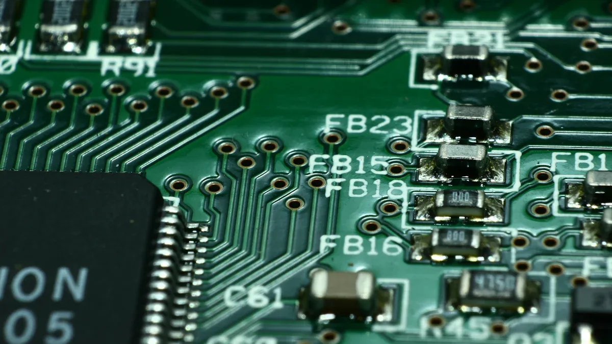
Industrial power board assembly uses several key technologies. Each technology supports different design requirements and impacts the performance and reliability of the final product. The choice of assembly method depends on the design, component type, and application needs.
| Technology Type | Components Description | Assembly Process Description | Advantages Description |
|---|
| Surface Mount Technology | Small, flat contacts or leads mounted on the PCB surface | Solder paste application, pick-and-place, reflow soldering | Space efficiency, higher component density, suitable for miniaturized devices |
| Through-Hole Technology | Components with wire leads inserted into pre-drilled holes | Manual/automatic insertion, solder applied on the opposite side, wave soldering | Strong mechanical connections are suitable for larger components requiring stability |
| Ball Grid Array (BGA) | An array of solder balls on the underside of the package | Placement on PCB, reflow soldering, X-ray inspection | High pin density, improved thermal performance, compact design |
Surface Mount Technology
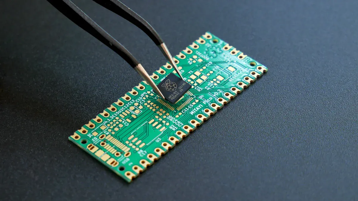
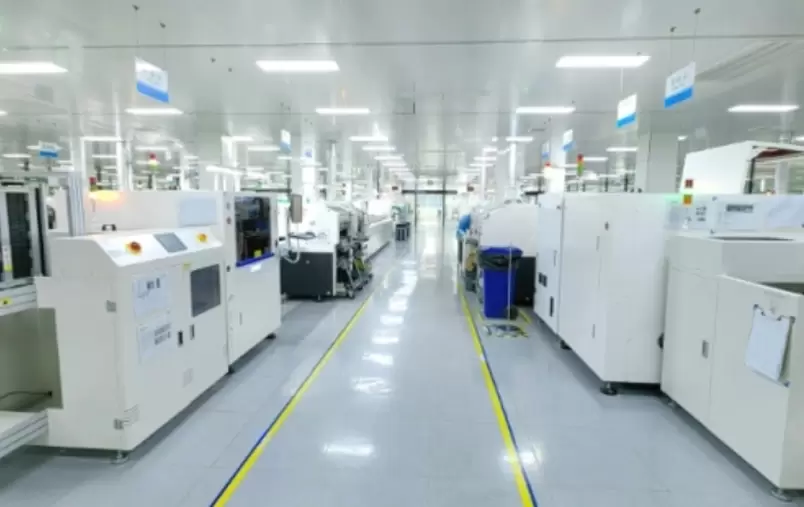
Surface mount technology dominates modern industrial power board assembly. This method places components directly onto the surface of the PCB, allowing for compact design and high component density. The process starts with careful design to ensure correct pad sizes and spacing. Automated pick-and-place machines position components with precision. Reflow soldering then secures the parts. Surface mount technology reduces board size and lowers production costs. However, it requires significant upfront investment and complex programming. Maintenance and flexibility also become important factors in the design phase.
Through-Hole Assembly
Through-hole technology remains essential for industrial power boards that demand strong mechanical connections. This method inserts component leads through holes in the PCB, then solder them on the opposite side. The design must account for hole placement and lead length. Through-hole technology is ideal for connectors, transformers, and other large parts that need stability. It increases durability and reliability, especially in harsh environments. Manual labor often plays a role, which can raise costs for low-volume production. The design process must balance these factors to achieve the desired performance.
Ball Grid Array
Ball grid array technology supports advanced design needs in industrial power boards. BGA packages use an array of solder balls on the underside, which connect to the PCB during reflow soldering. This approach allows for high pin counts and compact layouts. The design must ensure proper alignment and thermal management. BGA technology improves thermal performance and supports miniaturization. X-ray inspection checks for hidden defects after assembly. BGAs are critical for applications that require efficient use of space and high electrical performance.
Industrial Power Board PCB Assembly Process
The industrial power board PCB assembly process follows a series of precise steps. Each step in the process builds on the previous one to ensure high reliability and quality. Automation, careful design, and strict quality checks are essential throughout the process.
Design for Assembly
Design for assembly is the foundation of the PCB assembly process. Engineers focus on making the design simple and efficient. They select components that are easy to place and solder. They arrange parts to avoid crowding and to allow for automated placement. Good design for assembly reduces manufacturing costs and improves product quality. It also speeds up the process and increases reliability. When engineers use design for assembly, they see fewer defects and less rework. This approach leads to higher yields and more usable boards from each production run.
Benefits of design for assembly:●Reduced manufacturing costs
●Improved product quality
●Faster time-to-market
●Increased reliability
●Reduced rework and scrap
●Improved yields
Solder Paste Application
Solder paste application is a critical step in the industrial power board PCB assembly process. The process starts with cleaning the PCB to remove any contaminants. A precision stencil is made to match the design of the PCB pads. The stencil must be clean before use. Solder paste is applied using a squeegee, which spreads the paste evenly across the stencil openings. This ensures that the right amount of solder paste is deposited on each pad. After application, visual or automated optical inspection checks the accuracy of the solder paste placement.
Best practices for solder paste application:1. Design a precision stencil that aligns with SMT pads.
2 . Clean the stencil to remove any residual solder paste.
3.Apply solder paste using a squeegee to ensure even distribution.
4. Inspect solder paste application visually or with automated systems.
Proper solder paste application directly affects the quality of solder joints and the reliability of the final product.
Component Placement
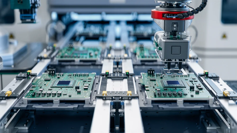
Component placement is the next step in the PCB assembly process. Automated pick-and-place machines position surface-mount components with high precision. These machines read the design files and place each part in the correct location. Automation reduces human error and increases the speed of the process. It also ensures that components are aligned properly, which is important for quality and reliability. For through-hole components, operators or machines insert the leads into the PCB holes. The design must allow for easy placement and alignment.
Advantages of automated component placement:●Reduces human error
●Increases assembly speed
●Ensures precise alignment
●Improves quality control
Soldering Methods
Soldering joins the components to the PCB. The industrial power board PCB assembly process uses several soldering methods, each with its own advantages. The choice depends on the design and the types of components used.
| Soldering Method | Advantages | Disadvantages |
|---|
| Wave Soldering | Fast and efficient for multiple connections, effective for through-hole components. | Not suitable for double-sided PCBs, as it can damage components on the underside. |
| Hand Soldering | Allows precise control, ideal for small production runs and repairs. | Labor-intensive and time-consuming, with potential for human error. |
| Reflow Soldering | Automated process with precise temperature control and consistent high-quality joints. | Requires specialized equipment; may not be suitable for all component types. |
| Selective Soldering | Targets specific areas, minimizes thermal stress on sensitive components. | A more complex setup may require additional programming. |
Reflow soldering is common for surface-mount components. It uses controlled heat to melt the solder paste and form strong joints. Wave soldering is used for through-hole parts, where the PCB passes over a wave of molten solder. Selective soldering targets specific areas, which helps protect sensitive components. Hand soldering is used for repairs or special cases.
Inspection & Testing
Inspection and testing are vital steps in the industrial power board PCB assembly process. These steps ensure that the PCB meets quality standards and works as designed. Multiple inspection points catch defects early and prevent faulty boards from reaching customers.
| Step | Description | Quality Assurance |
|---|
| Verify Parts | Check part numbers, quantities, and component conditions | Ensures no defects are present before assembly |
| PCB Cleaning | Remove contaminants that affect solder adhesion | Improves soldering quality |
| PCB Stencil Making | Create accurate stencils for solder paste application | Ensures precise solder paste placement |
| Solder Paste Printing | Apply solder paste to pads | Directly impacts soldering effectiveness |
| Visual/Optical Inspection | Check solder paste alignment | Ensures quality assembly |
| Pre-Reflow Inspection | Identify issues before soldering | Prevents defects |
| Reflow Soldering | Solder components with precise temperature control | Avoids soldering defects |
| Visual Inspection and AOI | Detect solder joint issues after soldering | Ensures reliability |
| DIP Insertion | Insert through-hole components | Ensures proper alignment |
| Visual Inspection (DIP) | Confirm through-hole solder joint integrity | Verifies reliability |
| Wave Soldering | Solder through-hole components | Ensures uniform soldering |
Advanced inspection techniques include automated optical inspection, in-circuit testing, flying probe testing, functional testing, BGA X-ray inspection, and environmental testing. These methods use cameras, probes, and even X-rays to check for defects and verify performance. Environmental testing exposes the PCB to temperature changes and vibration to ensure reliability in harsh conditions.
The industrial power board PCB assembly process relies on careful design, precise automation, and thorough quality checks. Each step builds on the last to create reliable and high-performance boards for industrial use.
Industrial Power Board Considerations
Reliability & Quality
Reliability stands as the most important requirement for industrial power board assemblies. These boards must operate for many years in harsh environments. The PCB fabrication process includes strict quality checks and robust testing to meet industry standards. Each industry has its own set of certifications that guide the fabrication and assembly process. The table below shows some common standards:
| Industry | Required Standards/Certifications |
|---|
| Automotive | IATF 16949, AEC-Q100 |
| Aerospace | AS9100, MIL-PRF-31032 |
| Medical | ISO 13485, FDA 21 CFR Part 820 |
| Military | MIL-PRF-55110, MIL-PRF-50884 |
| General Industrial | ISO 9001, UL 796 |
The PCB fabrication process for industrial boards often includes in-circuit testing, burn-in testing, and automated optical inspection. These steps help ensure that electrical reliability testing is thorough. Industrial PCBs are expected to last over 10 years, while consumer-grade boards may only last 2 to 5 years. Mastering every stage of fabrication, from design to testing, is essential for long-term reliability.
Thermal Management
Thermal management plays a key role in the performance and lifespan of industrial power boards. High temperatures can cause solder joint fatigue and layer delamination. Good thermal design spreads heat across the board and prevents hot spots. The following points highlight why thermal management matters:
●Prevents solder joint fatigue and layer delamination from temperature changes.
●Enhances reliability and extends the lifespan of the board in harsh environments.
●Uses power planes to spread heat and reduce thermal gradients.
The fabrication process must include steps for proper heat dissipation. This can involve thicker copper layers, larger pads, and careful placement of heat-sensitive components. Effective thermal management supports both reliability and safety.
High-Current Handling
High-current handling requires special attention during design and fabrication. Power integrity must be maintained to prevent interference and noise. Sensitive circuits should be isolated from power components. Good airflow and space for heat-sensitive parts are also important. Key considerations include:
●Design the power delivery network to minimize interference.
●Isolate sensitive circuits from high-current paths.
●Use full power and ground planes for better heat dissipation.
Large current spikes and voltage swings can disrupt board operation. The fabrication process must address these risks with robust electrical reliability testing and careful layout. Following standards like IPC-2221 and IEC 61000 ensures the board meets electrical and safety requirements.
Quality Assurance & Testing
Quality assurance and testing form the backbone of the PCB manufacturing process for industrial power boards. These steps ensure that each circuit board meets strict standards for reliability and safety. The manufacturing process uses a combination of advanced inspection methods and stress tests to detect defects before the printed circuit boards reach the field.
| Testing Method | Description |
|---|
| In-Circuit Testing (ICT) | Checks for shorts, opens, component values, and solder integrity. |
| Functional Testing | Validates the board's operation under real-world conditions. |
| Burn-In Testing | Subjects PCBs to elevated temperatures and voltages to detect early failures. |
| Automated Optical Inspection (AOI) | Detects visual defects post-assembly. |
In-Circuit Testing (ICT)
In-circuit testing is a key step in the PCB manufacturing process. This method tests each component and connection on the circuit board. ICT can detect open circuits, short circuits, and incorrect component values. The process also checks for solder joint defects and ensures electrical continuity. ICT identifies about 98% of faults by verifying each part one by one. This high level of accuracy helps manufacturers catch problems early and maintain high-quality PCBs. The PCB design process must support ICT by allowing easy access to test points.
ICT checks:●Open and short circuits
●Component placement accuracy
●Solder joint quality
Burn-In & Stress Testing
Burn-in and stress testing push printed circuit boards to their limits. During this phase, each circuit board operates under elevated temperatures and electrical loads for an extended period. The goal is to reveal early-life failures and ensure the board can withstand harsh conditions. Burn-in testing checks for component failures, solder joint integrity, and load capacity. This step is critical for industrial applications where reliability is non-negotiable. By identifying weak points before deployment, manufacturers reduce warranty claims and improve customer satisfaction.
Final Inspection
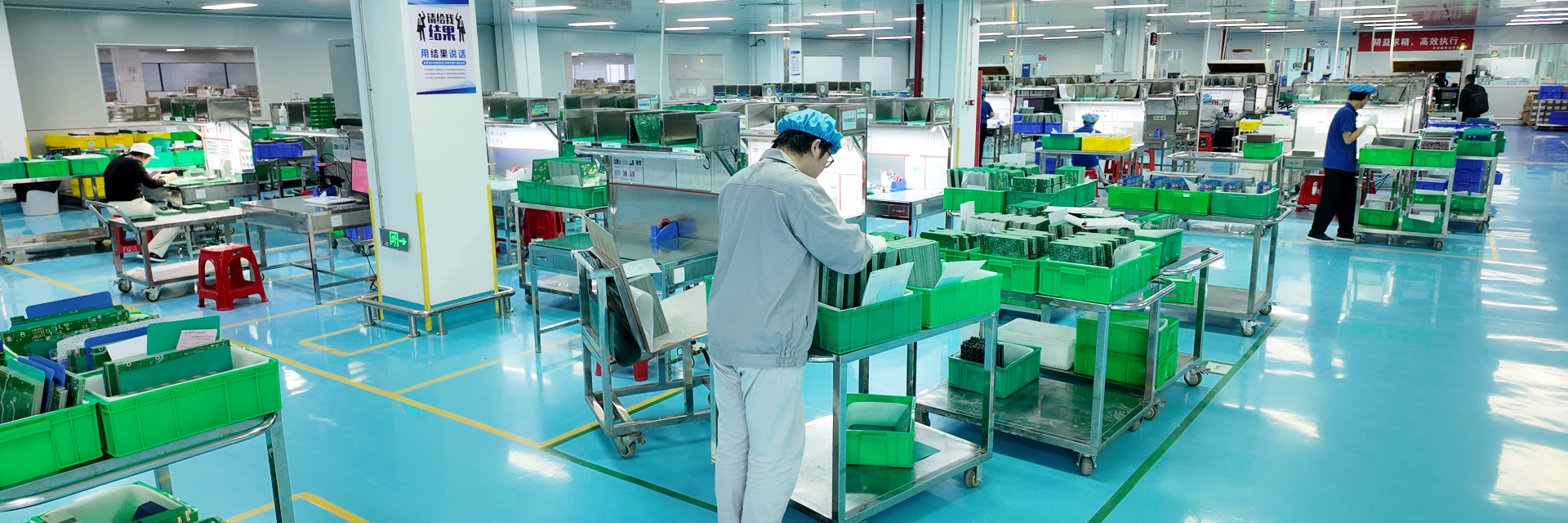
The final inspection is the last checkpoint in the PCB manufacturing process. Inspectors perform a thorough review of each circuit board to find physical and electrical flaws. This includes checking for missing components, solder defects, open circuits, and incorrect values. The process also verifies that the printed circuit board matches the original design. Any issues found during final inspection are corrected before the boards leave the factory. This step guarantees that only high-quality PCBs reach customers.
Common defects found:●Component misalignment
●Solder bridges
●Missing or incorrect parts
Quality control in the PCB manufacturing process ensures that every printed circuit board meets industry standards. These steps protect the performance and safety of industrial equipment, making quality assurance a vital part of the manufacturing journey.
The industrial power board PCB assembly process uses careful design, precise component placement, and advanced soldering methods. Each stage supports reliability and high performance. Testing methods like Functional Testing and Automated Optical Inspection help detect defects early. Quality assurance relies on strict standards and certifications.
| Certification/Standard | Purpose |
|---|
| ISO | Ensures quality products and services, enhancing credibility. |
| IPC | Develops quality standards for PCBs, ensuring reliability and quality. |
| RoHS | Limits hazardous materials, promoting environmentally friendly practices. |
These steps ensure every board meets industry requirements and performs safely in demanding environments.
About the author:

Sonic Yang
As a major in Electronics and Mechanical Automation, Sonic has been engaged in PCB design, R&D, and manufacturing of electronics for around 22 years, as the engineering director, and coordinates with the supply chain(components and CNC parts), providing professional support and consulting for global customers.

 en
en


 WhatsApp