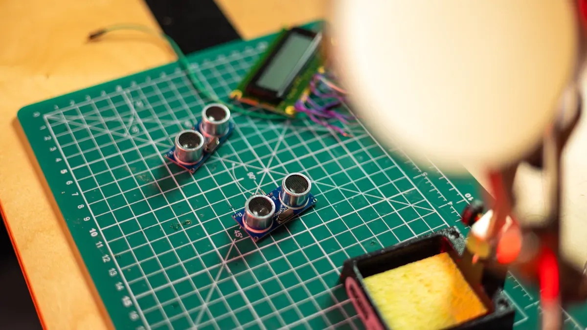
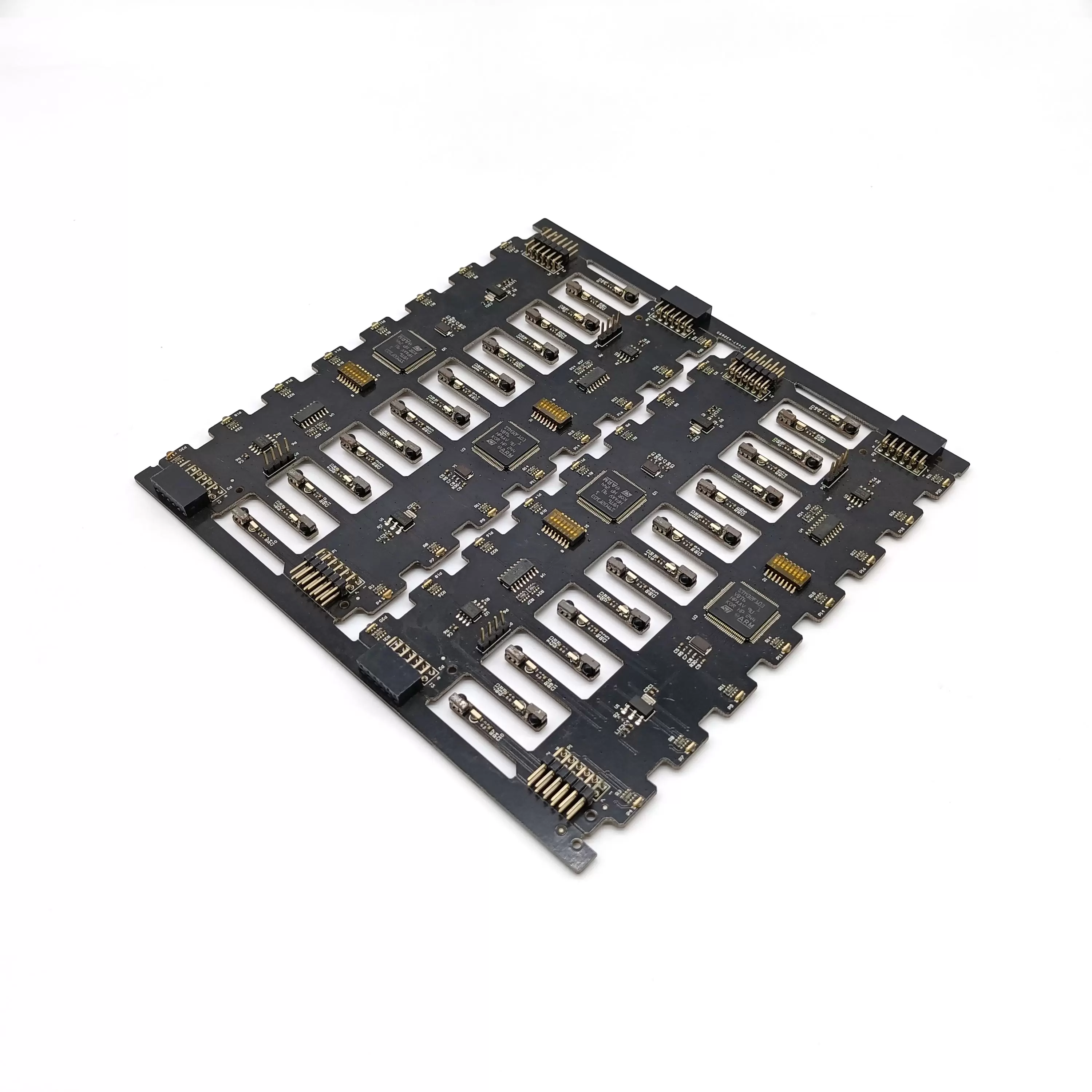
Flexible PCB technology appears everywhere, from smartphones and computers to automotive electronics and industrial IoT sensors. Many consumer products now rely on these advanced circuits, reflecting the high demand for compact and durable solutions. With 77% of Americans owning a smartphone, flexible PCBs have become essential in daily life. Anyone interested in diy electronics can create reliable circuits using simple tools and careful techniques. By following each step with attention, individuals can achieve professional results in their own workspace.
●Flexible PCBs are essential in modern electronics, offering compact and durable solutions for devices like smartphones and IoT sensors.
●Choosing the right materials, such as kapton for substrates, is crucial for ensuring flexibility and heat resistance in your PCB design.
●Proper cutting techniques, like laser cutting, help maintain the integrity of flexible substrates and prevent distortion during the manufacturing process.
●Applying adhesives or seed layers evenly is vital for strong bonding between copper foil and the substrate, ensuring reliable electrical connections.
●Drilling techniques must be chosen carefully to avoid damaging the flexible PCB; laser drilling offers precision for small holes.
●The etching process defines circuit traces; using fresh etching solutions and monitoring closely prevents common mistakes.
●Applying a coverlay protects the PCB from environmental factors and mechanical stress, enhancing durability and performance.
●Final inspections are essential to identify defects before assembly; thorough testing ensures the PCB functions correctly in its intended application.
Flexible PCB Materials and Tools
Flexible circuit boards require careful selection of materials and tools to ensure durability and performance. Each material serves a specific purpose in the manufacturing process. The right tools help achieve precise cuts, clean holes, and reliable electrical connections.
Essential Materials
Flexible substrate
Manufacturers often choose kapton as the primary substrate for flexible pcb projects. Kapton offers excellent heat resistance, high flexibility, and strong dimensional stability. Other substrates include polyester and liquid crystal polymer. The table below compares the most widely used materials for flexible circuit boards:
| Material | Heat Resistance | Flexibility / Bend Durability | Dimensional Stability | High-Frequency Electrical Performance | Moisture Resistance | Chemical Resistance | Process Compatibility | Cost Level | Typical Applications |
|---|
| Kapton (Polyimide, PI) | Excellent (>200°C) | Ideal for dynamic flexing | High | Good | Good | Excellent | Strong compatibility | Medium | Aerospace, automotive, medical |
| Polyester (PET) | Moderate (≤150°C) | Suitable for static use only | Average | Average | Poor | Moderate | Easy to process | Low | LED strips, membrane switches |
| Liquid Crystal Polymer (LCP) | Good (180–220°C) | Limited flexibility | High | Excellent | Excellent | Good | Requires controlled processing | High | 5G antennas, mobile RF modules |
| Polytetrafluoroethylene (PTFE) | Outstanding (>250°C) | Not suitable for bending | Moderate | Exceptional | Excellent | Excellent | Difficult to process | High | RF modules, microwave devices |
Kapton stands out for its ability to withstand repeated bending and high temperatures. Many hobbyists and professionals use copper clad kapton sheets for their flexible pcb designs.
Adhesive or seed coating
Adhesives bond the copper foil to the substrate. Seed coatings help with plating and improve adhesion. Kapton substrates often require specialized adhesives to maintain flexibility and heat resistance.
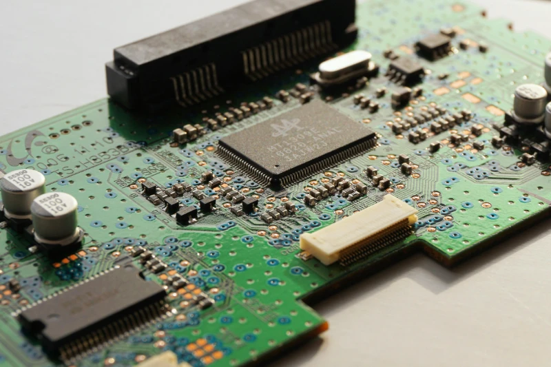
Copper foil
Copper foil forms the conductive layer. Manufacturers select foil thickness based on circuit requirements. Copper clad kapton combines the substrate and copper foil in one sheet, simplifying the process.
Etch-resist material
Etch-resist materials protect desired circuit patterns during etching. Common options include photoresist films and screen-printable inks.
Etching solution
Etching solutions remove unwanted copper. Ferric chloride and ammonium persulfate are popular choices. Users must handle these chemicals with care.
Coverlay or covercoat
Coverlay insulates and protects the finished circuits. Kapton-based coverlays provide flexibility and durability. Covercoats can also serve as solder masks.
Cleaning supplies
Cleaning supplies remove residues and ensure a smooth surface. Isopropyl alcohol, lint-free wipes, and brushes help maintain quality.
Required Tools
Drilling equipment
Drilling equipment creates holes for vias and component leads. Precision drills match hole diameters and board thickness. High-quality drills prevent tearing of kapton substrates.
Plating setup
Plating setups deposit metal layers inside drilled holes. Electroplating tanks and power supplies ensure reliable electrical connections.
Cutting tools
Cutting tools shape the flexible pcb. Routers, end mills, and V slot tools provide clean edges and accurate profiles. Disk or ring blades quickly divide boards into required sizes.
Safety gear
Safety gear protects users from chemicals and sharp tools. Gloves, goggles, and masks reduce risks during etching and drilling.
A clean workspace and proper safety equipment help prevent accidents and improve the quality of flexible circuit boards.
Substrate Preparation
Cutting Substrate
Sizing for your design
Flexible PCB manufacturing begins with precise substrate cutting. Engineers select the substrate size based on the circuit layout and component placement. Kapton sheets offer excellent flexibility and heat resistance, making them ideal for most designs. Maintaining flatness and tension control during cutting prevents distortion and ensures accurate registration. The table below compares common cutting methods for flexible PCB substrates:
| Cutting Method | Advantages | Disadvantages |
|---|
| Shearing / Guillotine | Fast and economical for simple panels. | Risk of delamination on delicate layers. |
| CNC routing | Good for medium complexity. | Produces clean edges with repeatable tolerances. |
| Laser cutting | Best for tight tolerances and complex shapes. | Minimizes mechanical stress on polyimide films. |
| Die punching | Efficient for high-volume single shapes. | Limited to simpler outline geometries. |
Laser cutting stands out for its ability to minimize mechanical stress on kapton substrates. CNC routing produces clean edges and repeatable tolerances, which suits medium complexity designs. Shearing works well for simple panels but may cause delamination. Die punching offers efficiency for high-volume production with simple outlines.
Applying Adhesive or Seed Layer
Even coating techniques
After sizing the substrate, technicians apply an adhesive or seed layer to bond copper foil to kapton. Several methods ensure strong adhesion and flexibility:
●Metallization and electroplating create a conductive seed layer on polyimide substrates. Electroplating follows, providing robust adhesion and flexibility.
●Casting on copper foil cures polyimide resin directly onto copper foil. This method delivers durability and stability, even in extreme conditions.
●Direct bonding of copper foil uses surface activation techniques. These methods enhance adhesion without traditional adhesives.
Uniform coating remains essential for reliable performance. Technicians use rollers, spray systems, or spin coaters to achieve even distribution. Surface activation methods, such as ion beam treatment or laser activation, improve the bond between copper and kapton. Chemical activation also increases reliability in demanding applications.
Copper Foil Lamination
Ensuring strong adhesion
Copper foil lamination forms the conductive layer of the flexible PCB. Industry standards recommend copper foil thicknesses of 12µm, 18µm, 35µm, and 70µm. The thickness influences current capacity, flexibility, heat dissipation, electromagnetic shielding, and mechanical reliability. Technicians select the appropriate thickness based on circuit requirements.
Best practices for strong adhesion include:
●Metallization techniques, such as sputtering and chemical vapor deposition, create a conductive seed layer on kapton substrates.
●Electroplating thickens the copper layer, ensuring dimensional stability and robust adhesion.
●Direct bonding involves casting and curing polyimide resin onto copper foil. This process eliminates adhesives and provides excellent thermal and chemical resistance.
●Surface activation methods, including ion beam and laser treatments, enhance the bond between copper and kapton.
Copper clad kapton simplifies lamination by combining the substrate and copper foil in one sheet. This approach reduces processing steps and improves reliability. Technicians must apply consistent pressure and temperature during lamination to avoid wrinkles and ensure uniform adhesion.
Drilling and Plating
Drilling Holes
Placement for components
Drilling holes in a flexible PCB allows for component mounting and electrical connections. Engineers must plan hole placement carefully to avoid stress points and ensure reliable performance. The substrate, often made from kapton, requires gentle handling to prevent tearing or distortion. Technicians mark the locations for vias and component leads based on the circuit layout. They use precise measurements to maintain alignment and spacing.
Several drilling techniques help minimize damage to flexible substrates. The table below compares common methods:
| Technique | Description | Advantages/Considerations |
|---|
| CNC Drilling | Utilizes CNC machines for drilling through-holes in flexible PCBs. | Suitable for multiple sheets, but requires careful monitoring of drill bit condition. |
| Micro-Punching | Involves punching holes in a roll format, suitable for mass production. | Limited to small hole diameters, slower than CNC drilling, but advancements have improved feasibility. |
| Laser Drilling | Uses lasers to create very small holes with minimal damage. | Can achieve extremely small diameters, but may be slower and more costly than other methods. |
Laser drilling stands out for its ability to create tiny holes starting at 0.1mm. This precision is crucial for high-density designs, where holes can be placed as close as 0.3mm apart. CNC drilling works well for double-sided flexible PCBs and allows for drilling multiple sheets at once. Micro-punching suits mass production but limits hole size and requires manual operation.
Through-Hole Plating
Ensuring electrical connectivity
Through-hole plating creates conductive pathways between layers of a flexible PCB. This step ensures that electrical signals travel reliably from one side to the other. Technicians clean the drilled holes to remove any debris or residues, especially when using laser drilling. Clean holes improve plating quality and reduce the risk of defects.
Reliable methods for through-hole plating include electroplating and chemical deposition. Electroplating deposits a thin layer of copper inside each hole, forming a strong electrical connection. Chemical deposition offers an alternative for smaller holes and complex designs. Both methods require careful control of solution concentration and plating time.
The table below summarizes the advantages and limitations of each drilling method for through-hole plating:
| Method | Advantages | Limitations |
|---|
| CNC Drilling | Suitable for multiple sheets, flexible options | Limited for smaller hole sizes, slower for mass production |
| Micro-Punching | Good for mass production, continuous process | Limited to hole diameters of 0.6–0.8 mm, longer process time |
| Laser Drilling | Can create very small holes (starting at 0.1mm) | High cost, slow speed, requires cleaning of residues |
Technicians often choose laser drilling for kapton substrates when high precision is required. They monitor the plating process to ensure uniform copper coverage and strong adhesion. Proper through-hole plating prevents open circuits and improves the reliability of flexible PCBs.
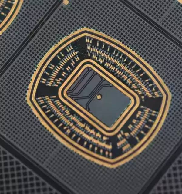
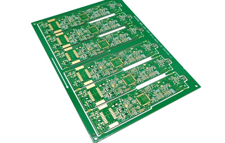
Flexible PCB Patterning
Etch-Resist Application
Printing or coating methods
Patterning forms the heart of any flexible pcb project. The process begins with applying an etch-resist material to the copper-clad kapton surface. This material protects the areas that will form the circuit traces during the etching stage.
Manufacturers use several types of etch-resist materials, each with unique advantages. The table below compares common options:
| Type of Etch-Resist | Graphics Manufacturing | Microvia Manufacturing | Manufacturing Accuracy | Manufacturing Taper Angle |
|---|
| Copper Etching Resist | Ordinary | Good | Good | 50°C - 60°C |
| Imageable Etching Resist Film | Easy | Ordinary | Ordinary | 40°C - 50°C |
Technicians select the appropriate method based on the design and complexity of the flexible pcb. For simple designs, screen printing or manual painting of resist works well. For higher precision, photoresist films allow for fine detail and repeatability.
The most effective techniques for applying etch-resist to flexible pcb surfaces include:
●Use advanced etching equipment and techniques. Precision spray etching systems provide better control and reduce the risk of damaging kapton.
●Optimize etchant chemistry. Milder etchants and careful temperature monitoring protect the flexible substrate while ensuring clean pattern transfer.
●Enhance handling protocols. Automated systems reduce manual handling and prevent mechanical stress on the kapton film.
●Test and validate designs. Small-batch tests help identify issues before full-scale production.
Etching Process
Removing unwanted copper
After applying the etch-resist, the next step involves removing unwanted copper from the kapton substrate. This process defines the final circuit traces and pads.
Common chemical solutions for etching copper in flexible pcb production include:
- Muriatic (HCl) acid
- 3% Hydrogen Peroxide
Technicians immerse the prepared board in the etching solution. The exposed copper dissolves, leaving only the protected areas intact. They monitor the process closely to avoid over-etching, which can undercut traces and weaken the flexible pcb.
Safety remains a top priority during etching. The table below outlines essential precautions:
| Safety Precaution | Description |
|---|
| Proper Ventilation | Ensures that harmful fumes are adequately dispersed, reducing inhalation risks. |
| Protective Gear | Essential for safeguarding workers from chemical exposure, including gloves and masks. |
| Environmental Considerations | Implementing closed-loop systems to recycle etchants minimizes waste and environmental impact. |
To achieve clean traces and avoid common mistakes, technicians should:
●Use fresh etching solution for each batch.
●Agitate the solution gently to ensure even copper removal.
●Rinse the board thoroughly with water after etching to stop the chemical reaction.
Stripping Etch-Resist
Cleaning the patterned board
Once the unwanted copper has been removed, the next step is to strip the etch-resist from the kapton surface. This reveals the finished copper traces and prepares the flexible pcb for further processing.
Recommended procedures for stripping etch-resist without damaging flexible pcb traces include:
- Chemical stripping uses solvents to dissolve the photoresist. This method is common and cost-effective, but technicians must avoid prolonged exposure to prevent damage to the kapton.
- Plasma stripping employs ionized gas to break down the resist material. This technique offers more precision and reduces chemical waste, making it suitable for delicate flexible pcb substrates.
- Laser stripping provides fast and precise removal of resist layers. It minimizes the risk of damage to the kapton and works well for complex circuit designs.
After stripping, technicians clean the board with isopropyl alcohol and lint-free wipes. This step removes any remaining residues and ensures a smooth, defect-free surface.
Careful patterning and cleaning help ensure that the flexible pcb maintains its electrical performance and mechanical flexibility. Proper handling of kapton throughout these steps prevents tears and preserves the integrity of the finished circuit.
Coverlay and Final Steps
Applying Coverlay
Protecting and insulating circuits
Technicians apply a coverlay to flexible PCBs to protect and insulate the copper circuitry. The coverlay serves several essential functions:
●Electrical insulation prevents short circuits by covering exposed copper traces.
●Mechanical protection shields the circuit from flexing, abrasion, and vibration.
●Environmental resistance guards against moisture, chemicals, and temperature extremes.
●The coverlay also protects copper from oxidation and contamination, forming a barrier against dust and air.
●It maintains flexibility, allowing the circuit to bend without cracking, and improves durability in harsh conditions.
Polyimide film, such as DuPont™ Kapton®, is the most common material for coverlay due to its flexibility, heat resistance, and strong insulation properties. Technicians use acrylic adhesives for flexibility or epoxy adhesives for higher heat resistance to bond the coverlay to the copper circuitry.
Best practices for applying coverlay include several key steps:
1.Clean the bare circuit surface thoroughly to remove dust and residues.
2.Pre-cut the polyimide film and create openings for pads and vias.
3.Align the coverlay carefully with the copper traces to ensure proper coverage.
4.Laminate the coverlay using heat and pressure in a vacuum press.
5.Cure the adhesive fully to achieve a strong bond.
6.Inspect the lamination for alignment and bonding quality.
Technicians match adhesive thickness to copper thickness for proper sealing and size openings carefully to maintain protection. They allow for registration tolerance to prevent defects and avoid stress points in active bend areas to improve fatigue life.
Cutting and Shaping
Trimming to final dimensions
After lamination, workers cut and shape the flexible PCB to its final dimensions. This step ensures the board fits its intended form factor and can accommodate dynamic bending, which is important for applications like wearable electronics or foldable displays.
Several methods help achieve precise results:
●Steel rule dies cut complex shapes with an accuracy of ±0.1mm.
●Routing works well for straight edges, achieving an accuracy of ±0.2mm.
●Workers remove extra tabs and use light scores to mark fold lines.
During this phase, technicians prepare the PCB for final testing and assembly. They ensure the board meets quality, flexibility, and electrical performance standards.
Final Inspection
Checking for defects
Final inspection ensures the flexible PCB meets all quality standards before assembly. Technicians perform several quality control steps:
1.Visual inspection detects physical defects. Workers use magnification tools for manual checks and automated optical inspection (AOI) systems for a wide range of defects.
2.Automated X-ray inspection (AXI) identifies hidden defects, such as internal cracks or voids.
3.Automatic laser tests (ALT) measure critical PCB dimensions for accuracy.
Common defects found during inspection include:
●Solder bridging, which occurs when excess solder creates unintended connections between pads.
●Plating voids, which are gaps in copper plating caused by contaminated drilling debris.
●Non-wetting solder joints, which result from oxidized PCB surfaces and lead to weak connections.| Defect | Causes | Prevention |
|---|
| Solder Bridging | Excess solder paste | Use proper solder mask design |
| Plating Voids | Contaminated drilling | Thorough pre-plating cleaning |
| Non-Wetting Solder Joints | Oxidized PCB surfaces | Proper humidity-controlled storage |
Technicians correct solder bridging by removing excess solder and reapplying under controlled conditions. They clean solder balls with isopropyl alcohol and optimize reflow conditions. For insufficient wetting, they apply additional flux and ensure proper surface preparation.
A thorough inspection process helps guarantee that the flexible PCB will perform reliably in its final application.
Assembly and Testing
Soldering Components
Techniques for flexible substrates
Soldering components onto a flexible PCB requires careful technique to protect the delicate substrate. Flexible circuits can warp or delaminate if exposed to excessive heat or mechanical stress. Technicians follow several best practices to achieve reliable solder joints:
●Preheat the board with a hot plate set between 60°C and 80°C. This step reduces thermal shock and prevents moisture from causing delamination.
●Apply flux to both the pad and the component lead. Flux improves wetting and helps solder flow smoothly.
●Tin the pad lightly before placing the component. This action ensures a quick bond and reduces the time the iron contacts the board.
●Place the component and apply heat for only 2–3 seconds. Prolonged heating can lift pads or damage the substrate.
●Feed solder to form a smooth fillet, avoiding overheating.
●Use low-temperature solder pastes, such as Sn42/Bi58, which melt at approximately 138°C. These solders minimize thermal stress on the flexible material.
●Support the board with a rigid carrier or fixture to prevent bending during soldering.
●Keep the soldering iron temperature below 300°C and minimize contact time to less than 3 seconds per joint.
●Use Kapton tape or fixtures to hold components in place.
●Clean any corrosive flux residues with isopropyl alcohol after soldering.
Common challenges during soldering include delamination, lifted pads, cold solder joints, warping, and cracked joints. Technicians address these issues by pre-baking circuits, using the lowest effective temperatures, limiting dwell time, and supporting the board properly. They also design solder joints in non-flex areas and may apply conformal coating to protect against mechanical stress.
Testing the Flexible PCB
Continuity and functionality checks
After assembly, technicians test the flexible PCB to ensure all connections work as intended. Several methods help verify electrical continuity and overall functionality:
| Testing Method | Description |
|---|
| Flying Probe Test | Uses pogo-pin based probes to inject and monitor signals via test pins on the boards. |
| Functional Test | Verifies that the PCB works as intended in a real-world environment, ensuring all components function together. |
| Manual/Visual Testing | Involves visual inspections to identify cosmetic and process defects, often used for simpler assemblies. |
Technicians often start with continuity tests using a multimeter. They check for open circuits, shorts, and proper resistance values. Impedance tests may follow for high-speed circuits. Functional tests confirm that the assembled board performs as designed under real-world conditions.
If a flexible PCB fails continuity or functionality tests, technicians follow a systematic troubleshooting process:
●Visual inspections help identify signs of overheating, bulging, or discoloration on components.
●Continuity testing with a multimeter locates electrical faults by checking voltage and resistance.
●Advanced inspection techniques, such as X-ray or microscopic analysis, reveal hidden defects like internal cracks or poor solder joints.
For advanced projects, technicians may use automated optical inspection (AOI) or X-ray inspection for higher accuracy. Those seeking professional results can explore contract assembly services or invest in specialized equipment for mass production.
About the auther:

Sonic Yang
As a major of Electronics and Mechanical Automation, Sonic has been engaged in PCB design, R&D, manufacturing of eletronics for around 22 years, as engineering director and coordinates with supply chain(components&CNC parts), providing professional supports and consults for global customers.
 en
en


 WhatsApp