A pcb refers to an empty circuit board, while PCB assembly PCB assembly service PCB assembly China delivers a completed board with all components installed. This difference remains essential when sourcing electronics manufacturing in China. Key impacts on supplier selection include:
●The need to choose between pcb fabrication experts or assembly providers
●Effects on cost and lead times
●Required technical expertise for each process
PCB vs. PCBA: Core Differences
What Is a PCB?
Bare Board Structure
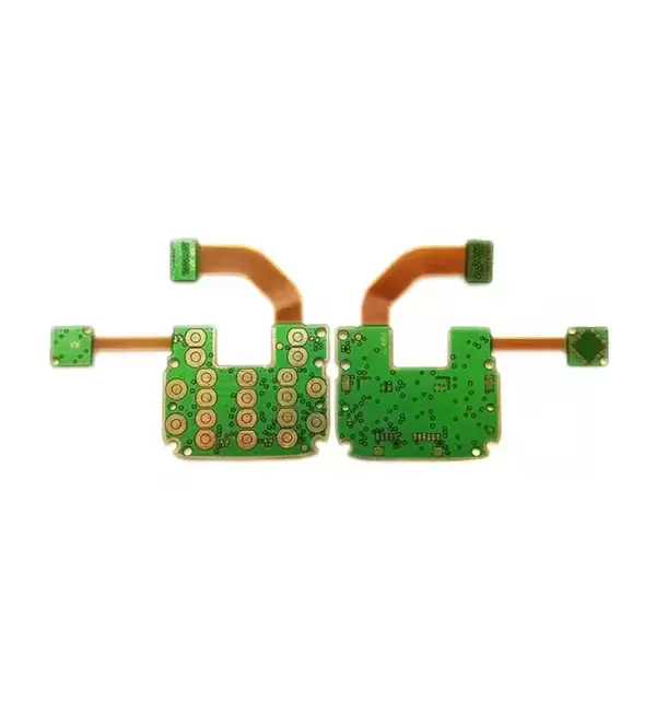
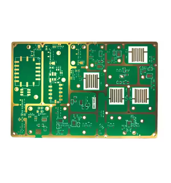
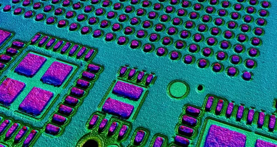
A printed circuit board, often called a pcb, forms the foundation of most electronic devices. This circuit board consists of layers of substrate material, such as fiberglass, and copper traces that create pathways for electrical signals. The structure remains rigid and flat, designed to support and connect electronic components in a precise layout.
No Components Attached
A pcb leaves the factory as a bare board. No electronic components appear on its surface. Manufacturers produce these boards to exact specifications, but at this stage, the circuit board cannot perform any electronic function. It simply serves as a platform for future assembly.
What Is PCBA?
Assembled Components
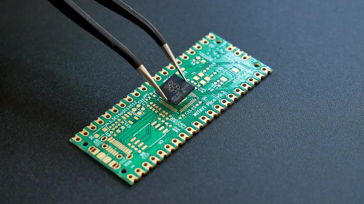
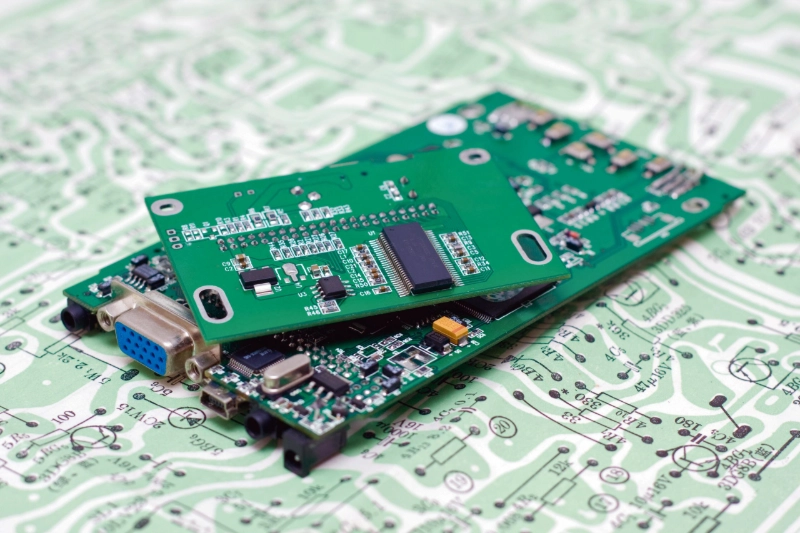
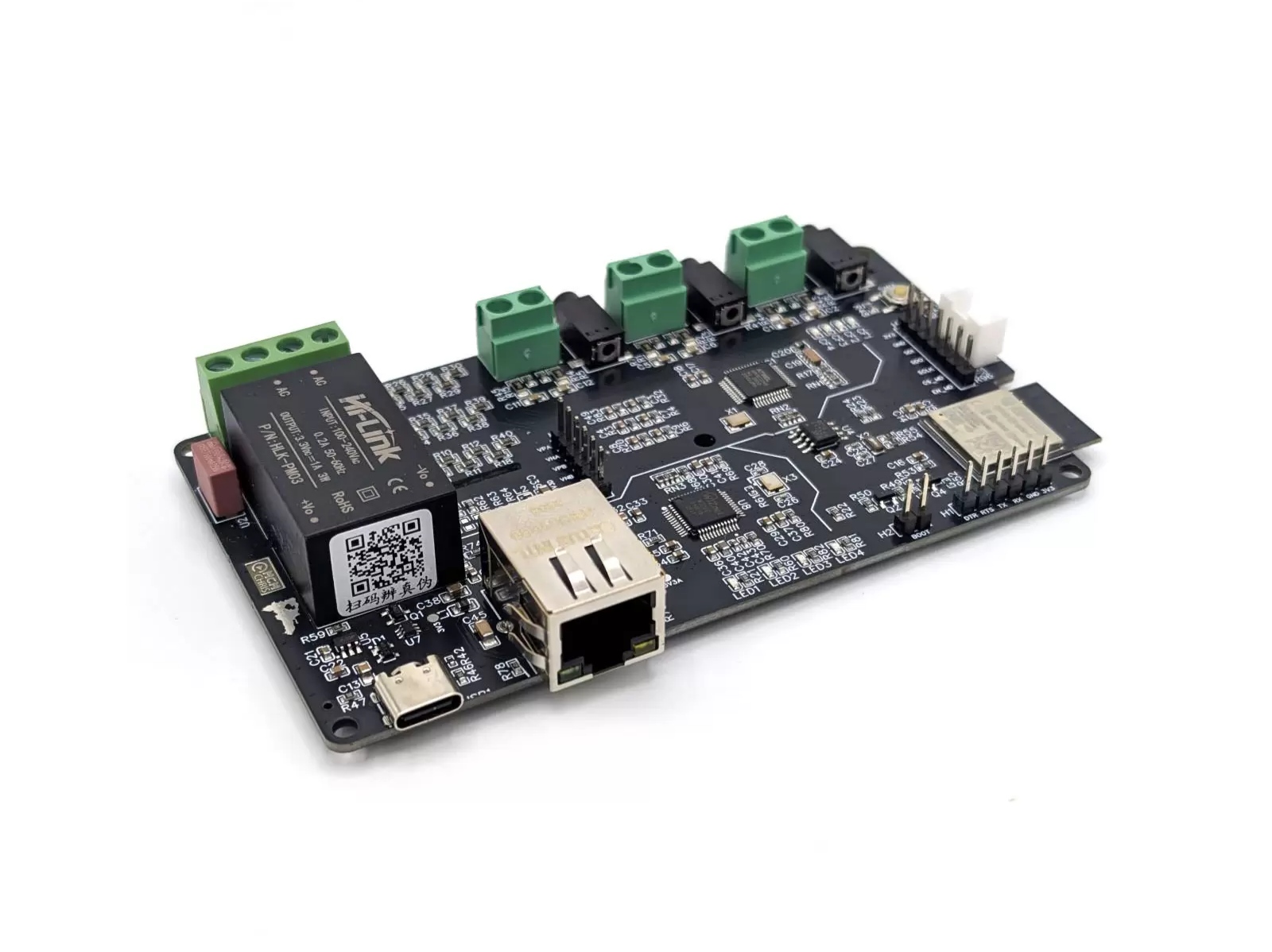
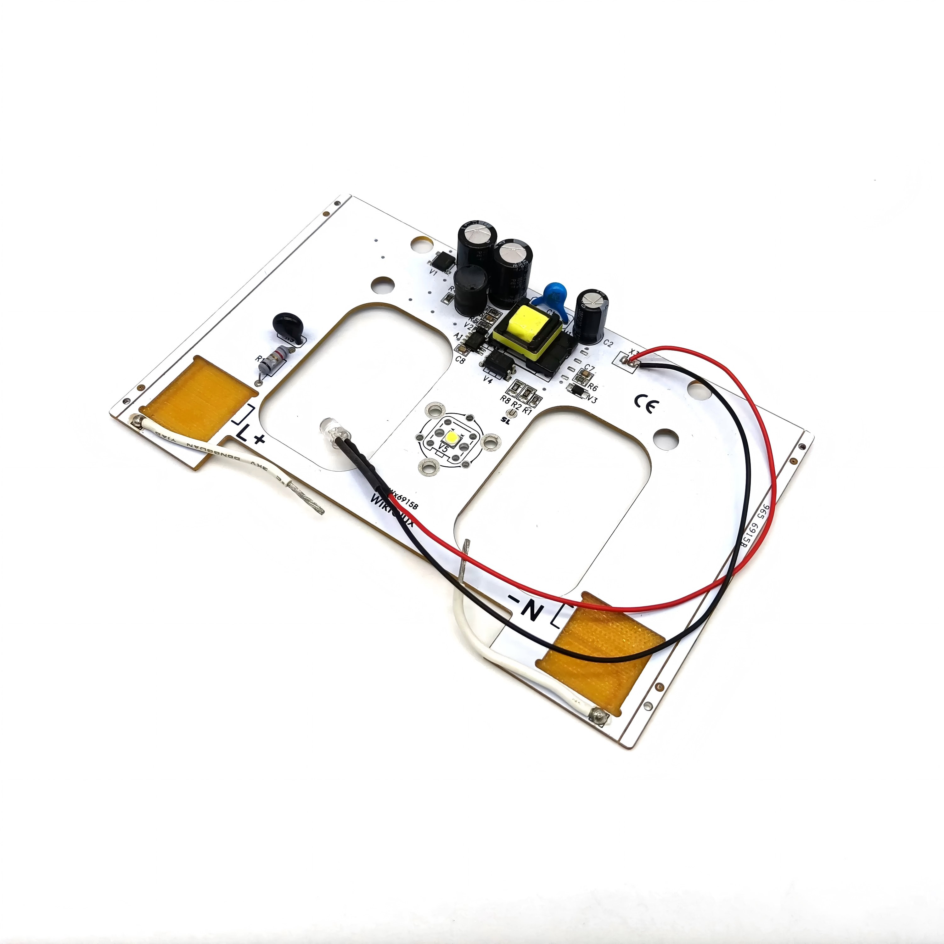
PCBA stands for printed circuit board assembly. This term refers to a pcb that has undergone the assembly process, where skilled technicians or automated machines place and solder electronic components onto the board. These components include resistors, capacitors, integrated circuits, and connectors.
Ready for Use
Once assembly finishes, the pcba becomes a functional unit. It can be installed directly into electronic products, from smartphones to industrial equipment. The completed assembly ensures the circuit board performs its intended role within a device.
Key Distinctions
The differences between a pcb and a pcba go beyond appearance. They involve structure, function, process, and application. The following table summarizes the technical definitions according to international electronics manufacturing standards:
| Term | Definition |
|---|
| PCB | A blank board that serves as the foundation of electronic devices, made of laminate material with conductive pathways for connecting components. |
| PCBA | A completed assembly of a PCB that includes all necessary electronic components for functionality. |
A closer look at their features highlights further distinctions:
| Feature | PCB | PCBA |
|---|
| Definition | The foundation of electronic devices, consisting of substrate material and copper traces. | A pcb that has undergone assembly with electronic components soldered onto it. |
| Functionality | Does not function on its own; serves as a base for components. | A complete, functional unit ready for installation in a product. |
| Assembly Process | Not assembled; just the bare board. | Involves Surface Mount Technology (SMT) or Through-Hole Technology (THT). |
| Component Placement | No components present. | Components are soldered onto the board. |
| Equipment Required | None required for pcb. | Requires specialized equipment like pick-and-place machines and reflow ovens. |
Application Areas
The electronics industry uses both bare pcbs and assembled pcbas for different purposes. Bare circuit boards often appear in prototyping and educational settings, where engineers and students test new designs. Assembled pcbas dominate commercial production, powering everything from consumer electronics to medical devices.
| Application Area | Bare PCBs Applications | Assembled PCBAs Applications |
|---|
| Consumer Electronics | Prototyping and customization for devices like smartphones and tablets | Fully assembled for mass production of devices |
| Automotive Industry | Used in basic components like windshield wipers | Advanced systems for safety and navigation |
| Medical Devices | Prototyping for educational purposes | Fully assembled for critical medical equipment |
| Industrial Equipment | Custom designs for specific industrial applications | High-volume production for robust industrial systems |
| Telecommunications | Basic prototypes for testing communication devices | Fully assembled for reliable communication systems |
| Aerospace Industry | Custom designs for specialized applications | Assembled for high-reliability aerospace systems |
●Bare pcbs support hands-on learning and design iteration.
●Assembled pcbas offer quality, speed, and cost-effectiveness for large-scale production.
Cost and Turnaround Time
Manufacturing a pcb involves material and processing costs, which typically account for 20% to 30% of the total cost. For pcba, component procurement becomes the largest expense, often reaching 40% to 60% of the total. In China, pcb production can take as little as 24 hours for rush prototypes, while complex boards may require six weeks or more. PCBA services can match quick turnaround times for simple jobs, but standard lead times range from one to three weeks.
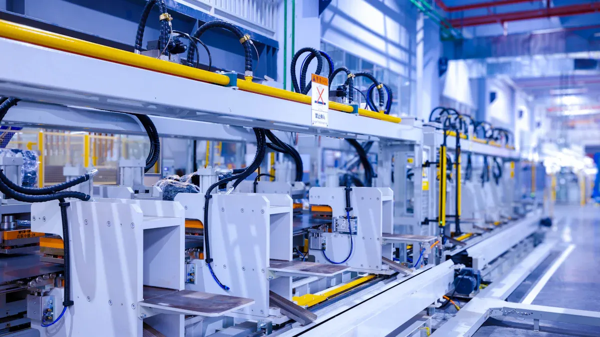
PCB Production Process
The pcb manufacturing processes in China follow strict industry standards to ensure reliability and performance. Each step transforms raw materials into a precise, functional circuit board. The process involves advanced technology, skilled labor, and rigorous quality control.
Fabrication Steps
Material Layering
Manufacturers begin by selecting the appropriate base material. FR-4 remains the most common choice due to its excellent electrical insulation, mechanical strength, and heat resistance. Other materials, such as Rogers and PTFE, serve specialized applications. The production team stacks layers of substrate and copper foil to form the core structure.
●FR-4: Flame retardant laminate, suitable for general applications.
●Copper Foil: Provides conductive pathways for electrical signals.
●Solder Mask: Protects the pcb and prevents solder bridges.
●Rogers: Used for radio frequency circuits with low dielectric loss.
●PTFE: Ideal for high-frequency circuits.
●Polyimide: Offers flexibility and heat resistance for dynamic environments.
The thermal properties of these materials play a critical role. Glass Transition Temperature (Tg) indicates when the material softens. Decomposition Temperature (Td) marks the point where the material breaks down. The Coefficient of Thermal Expansion (CTE) measures how much the material expands with temperature changes. These factors ensure the pcb can withstand demanding operational conditions.
| Material Type | Properties |
|---|
| FR-4 | Excellent electrical insulation, mechanical strength, heat resistance. |
| Copper Foil | Conductive pathways for routing electrical signals and power distribution. |
| Solder Mask | Protective layer, prevents solder bridges, protects against corrosion. |
| Silkscreen | Printed text and symbols for assembly and identification. |
| Rogers | Low dielectric loss, excellent signal integrity, controlled impedance. |
| PTFE | Exceptional performance in high-frequency applications. |
| FR-2 | Moderate electrical insulation, lower mechanical strength. |
| Polyimide | Flexible, withstands high temperatures, good electrical insulation. |
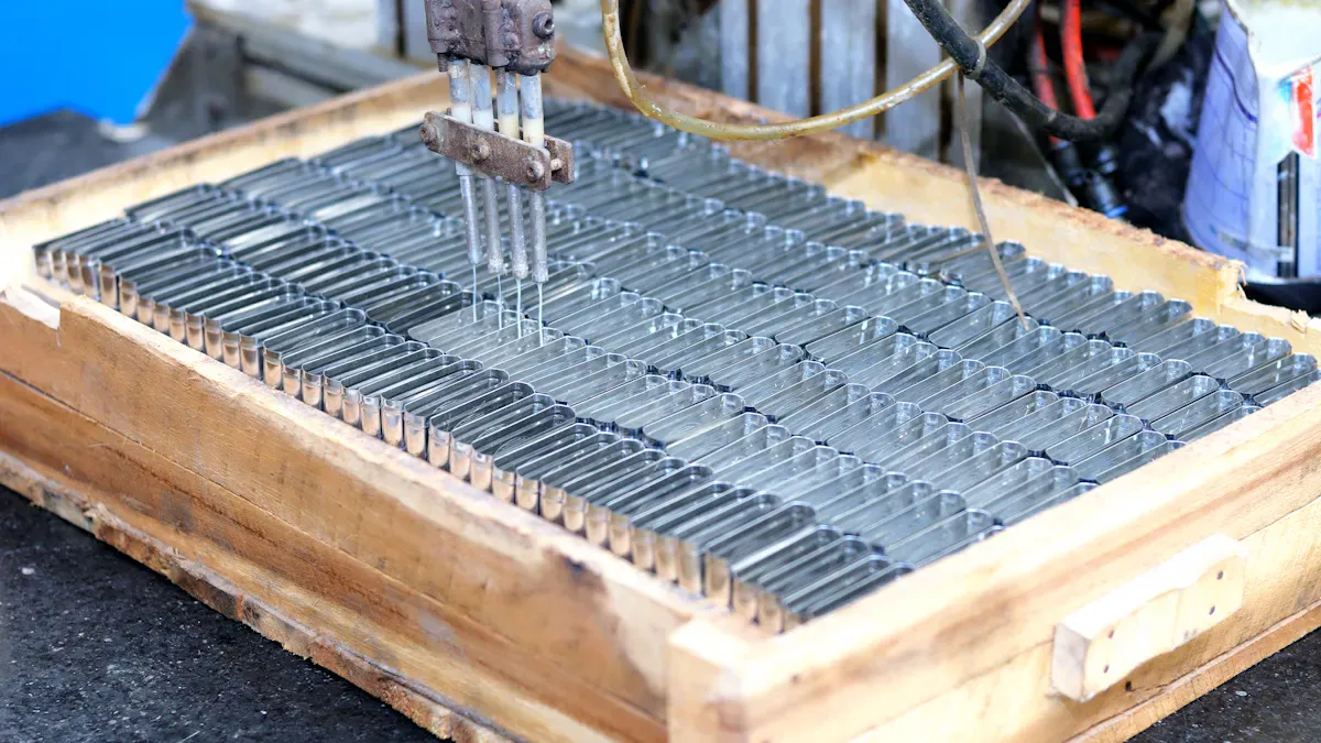
Etching and Drilling
After layering, the pcb moves to the etching and drilling stage. The design undergoes a Design for Manufacture (DFM) check to ensure compatibility with production capabilities. Engineers review the design for errors and approve it for printing. A specialized plotter printer creates a film of the pcb layout, using different inks for circuits and non-conductive areas.
The next step involves applying a photo-sensitive film to the copper layers. Ultraviolet light hardens the resist in the desired pattern. Unhardened areas are removed, and the exposed copper is etched away, leaving only the required circuitry. Precision drilling machines create holes for component leads and vias, ensuring accurate alignment.
1.Design for Manufacture (DFM) Check
2.Design Review
3.Printing of the PCB Design
4.Printing the Copper for Interior Layers
Surface Preparation
Surface preparation ensures the pcb is ready for assembly or further processing. Technicians clean the board to remove contaminants. They apply a solder mask to protect the copper traces and prevent solder bridges during assembly. Silkscreen printing adds text and symbols for identification and guidance.
Regular audits and inspections play a vital role in maintaining pcb quality. These checks help manufacturers identify defects early, reducing material waste and preventing costly rework. This proactive approach keeps production on schedule and minimizes delivery delays.
Output: Bare PCB
The final output of these pcb manufacturing processes is a bare pcb. This board contains all the designed copper traces, drilled holes, and protective layers but no electronic components. It serves as the essential platform for future assembly.
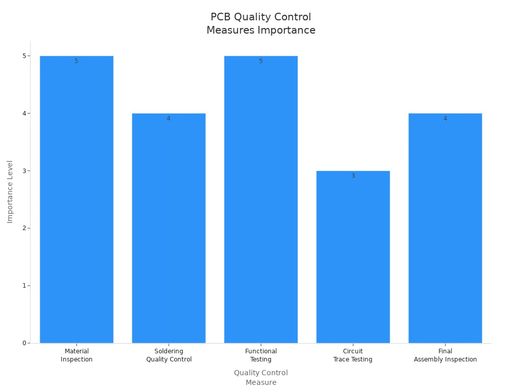
Quality control remains a top priority throughout production. The following table highlights common quality control measures, their importance, and the return on investment:
| Quality Control Measure | Importance Level | Cost Related to Quality Improvement | Expected Benefit | Return on Investment |
|---|
| Material Inspection | 5 | $2,000 | $10,000 | 400% |
| Soldering Quality Control | 4 | $1,500 | $7,500 | 400% |
| Functional Testing | 5 | $3,000 | $12,000 | 300% |
| Circuit Trace Testing | 3 | $1,200 | $4,800 | 300% |
| Final Assembly Inspection | 4 | $1,800 | $6,000 | 233% |
The bare pcb leaves the factory ready for assembly, prototyping, or direct shipment to customers. High standards in pcb manufacturing processes ensure consistent quality and reliable performance for every application.
PCB Assembly Service in China
What Is PCB Assembly?
PCB assembly refers to the process of mounting electronic components onto a pcb to create a functional printed circuit board assembly. Chinese manufacturers offer pcb assembly pcb assembly service pcb assembly china that transforms bare boards into completed pcb assembly units ready for integration into electronic products. This service includes sourcing components, mounting them using advanced techniques, and performing rigorous quality checks. Companies in China specialize in pcb assembly processes that deliver high-quality results for industries ranging from consumer electronics to automotive and medical devices.
PCB Assembly Service Steps
Chinese providers follow a systematic approach to pcb assembly. Each step ensures precision and reliability in the finished product.
Component Sourcing
Manufacturers source components from trusted suppliers. They select parts based on customer specifications, ensuring compatibility and quality. The availability of materials in China supports economies of scale, which reduces costs and streamlines procurement.
SMT & Through-Hole Mounting
Surface Mount Technology (SMT) and Through-Hole Technology (THT) represent the main methods for mounting components. SMT places parts directly onto the pcb surface using automated machines. THT involves inserting component leads through holes in the board and soldering them for secure attachment. Chinese factories use both techniques to meet diverse design requirements.
Soldering & Inspection
Soldering joins components to the pcb using wave soldering or reflow soldering. Skilled technicians and automated systems ensure strong electrical connections. Inspection follows soldering, using visual checks, Automatic Optical Inspection (AOI), and X-ray inspection to detect defects. Functional testing confirms that the completed pcb assembly operates as intended.
| Step | Description |
|---|
| Solder Paste Stenciling | Application of solder paste on the pcb using a stencil to prepare for component mounting. |
| Component Mounting | Placement of components on the pcb, either manually or using automated systems. |
| Soldering | Joining components to the pcb using wave soldering or reflow soldering techniques. |
| Inspection | Quality checks using visual/manual inspection, AOI, or X-ray inspection. |
| Functional Testing | Testing the assembled pcb for functionality and performance after assembly. |
Why Choose PCB Assembly China
Chinese pcb assembly pcb assembly service pcb assembly china offers several advantages over other regions. Companies benefit from lower labor costs, advanced manufacturing facilities, and reliable material availability.
| Advantage | Description |
|---|
| Availability of materials | China has a significant share of essential materials, facilitating economies of scale. |
| Manufacturing facilities | Well-equipped facilities in China enable efficient pcb manufacturing and assembly. |
| Labor cost | Overall costs, including labor, are lower in China compared to the USA, making it cost-effective. |
Chinese pcb assembly pcb assembly service pcb assembly china delivers expertise, cost savings, and rapid turnaround for global clients. Companies seeking completed pcb assembly benefit from streamlined pcb assembly processes and reliable quality control.
Differences Between PCBA and PCB
Process Comparison Table
The differences between pcba and pcb become clear when examining their processes side by side. The following table outlines the main distinctions in definition, function, complexity, and production requirements:
| Aspect | PCB (Bare Board) | PCBA (Assembled Board) |
|---|
| Definition | Raw board with copper traces, pads, no components | PCB with mounted electronic components |
| Functionality | Inert; enables connections, performs no action | Active circuit, performs electronic functions |
| Fabrication Process | Etching, drilling, plating, coating | Component placement, soldering, inspection |
| Complexity | Based on layer count and design | Based on component density and technology |
| Design | CAD layout | Component sourcing, DFM checks |
| Testing Requirements | Physical inspection only | Functional testing, AOI, X-Ray, in-circuit |
| Cost | Lower (materials, fabrication only) | Higher (components, labor, testing) |
| Lead Time | Faster turnarounds | 2-4 week cycles |
| Applications | Serves as base for assembly | Powers electronic devices |
This comparison highlights how the differences between pcba and pcb affect every stage of electronics manufacturing.
Inputs and Outputs
PCB fabrication and pcba assembly require different materials and produce distinct outputs. The input materials for pcb fabrication include copper foil and insulating substrates such as FR-4. The output is a bare circuit board, which cannot function until further assembly. In contrast, pcba assembly uses fabricated boards and electronic components as inputs. The output is a functional circuit ready for integration into electronic products.
| Process | Input Materials | Output Products |
|---|
| PCB Fabrication | Copper foil, insulating substrate (FR-4) | Bare circuit board |
| PCB Assembly | Fabricated PCB, electronic components | Functional circuit board |
●PCB fabrication involves layering materials, etching copper traces, drilling holes, and applying surface finishes.
●PCBA assembly involves mounting and soldering components onto the board, followed by inspection and testing.
Skills and Equipment
PCB production and pcba assembly require different skill sets and specialized equipment. Technicians in pcb fabrication operate machines for etching, drilling, and plating. They must understand material properties and quality control standards. PCBA assembly demands expertise in component placement, soldering, and advanced inspection methods. Operators use pick-and-place machines, reflow ovens, and automated optical inspection systems.
Key skills and equipment for each process include:
PCB Fabrication:
●Skills: Material handling, precision drilling, quality inspection
●Equipment: Etching machines, CNC drills, plating lines
PCBA Assembly:
●Skills: Soldering, component placement, functional testing
●Equipment: Pick-and-place machines, reflow ovens, AOI and X-ray systems
The right combination of skills and technology ensures reliable performance and high-quality output at every stage.
Choosing PCB Production or Assembly
Project Needs Assessment
Every electronics project begins with a clear assessment of requirements. The project scope determines whether pcb production or pcba assembly is necessary. Engineers must evaluate the complexity of the circuit, the volume of boards needed, and the intended application. The quality of pcb boards plays a critical role in the reliability of the final product. Selecting a manufacturing service with proven durability and accuracy ensures the project meets industry standards. Teams should also review the assembly capabilities of potential suppliers. The expertise and equipment of a pcb assembly company influence the efficiency and scalability of the process.
●Assess the technical demands of the design.
●Determine if the project requires bare pcb boards or fully assembled pcba units.
●Review the supplier’s manufacturing and assembly capabilities.
Quality, Lead Time, and Cost
Quality standards and certifications remain essential when selecting pcb or pcba services in China. Manufacturers often hold certifications such as ISO 9001, IPC-A-610, and RoHS, which guarantee adherence to rigorous quality management and environmental regulations. The following table summarizes key certifications for different industries:
| Certification | Description |
|---|
| ISO 9001 | Quality Management System standard. |
| IATF 16949 | Required for automotive manufacturing. |
| ISO 13485 | Essential for medical device production. |
| AS9100D | The benchmark for aerospace quality. |
Lead times and costs vary based on order volume. Large volume orders benefit from lower labor and material costs, creating significant savings. Small volume orders often incur higher per-unit costs due to setup fees. Prototyping in China is typically 10-20% cheaper than in the USA. For example, a 6-layer pcb costs $15 in China compared to $18 in the USA. Labor-intensive processes such as assembly and inspection are more affordable in China, especially for high-volume production. Tooling costs remain low due to competitive subcontractor networks.
●Large orders offer economies of scale and faster lead times.
●Small orders face higher setup fees but competitive turnaround.
●Labor and material costs in China provide cost advantages for both pcb and pcba services.
Supplier Selection Tips
Choosing a reliable pcb or pcba supplier in China requires careful evaluation. Industry experience, areas of expertise, and production scale should guide the selection process. Manufacturers with more than five years of experience often deliver consistent results. Certifications such as ISO9001, ISO14001, ISO13485, and UL indicate a commitment to quality. Client testimonials provide insight into the supplier’s reliability. Additional services like pcb design, assembly, and testing add value.
| Criteria | Description |
|---|
| Industry Experience | Prefer manufacturers with 5+ years of experience in the PCB industry. |
| Areas of Expertise | Ensure the manufacturer specializes in the type of PCB you need. |
| Scale of Production | Check if the manufacturer can handle your required production scale. |
| Certifications | Look for necessary certifications like ISO9001, ISO14001, ISO13485, and UL. |
| Testimonials | Review client testimonials to verify the manufacturer's claims. |
| Additional Services | Consider manufacturers that offer extra services like PCB design, assembly, and testing. |
●Quality assurance standards such as ISO 9001 and IPC-A-610 ensure rigorous quality control.
●Inspection and testing capabilities, including AOI and X-ray, confirm product reliability.
●Effective communication and customer support reflect the supplier’s professionalism.
Sourcing PCB Assembly China: Best Practices
Evaluating Providers
Selecting the right partner for pcb assembly in China requires a structured approach. Companies should focus on several critical factors to ensure reliable outcomes:
1.Industry Experience: Providers with over five years in the field demonstrate stability and expertise.
2.Areas of Expertise: Manufacturers must specialize in the specific type of pcb required for the project.
3.Scale of Production: The provider should match the client’s production volume, whether for prototypes or mass manufacturing.
4.Certifications: Recognized certifications such as ISO9001 and ISO14001 indicate strong quality management systems.
5.Testimonials: Client feedback offers insight into the provider’s credibility and service quality.
6.Additional Services: Value-added offerings like pcb design, assembly, and testing streamline the supply chain.
7.Communication: Clear and responsive communication prevents misunderstandings and project delays.
8.Turnaround Time: Providers must commit to realistic deadlines and deliver on time.
9.Pricing: Transparent pricing helps balance cost and quality, avoiding unexpected expenses.
A thorough evaluation of these factors helps companies identify trustworthy pcb assembly partners in China.
Common Challenges
Sourcing pcb assembly from China presents several challenges that can impact project success:
●High costs may reduce profit margins, especially for complex or low-volume orders.
●Long lead times can delay product launches and disrupt schedules.
●Inconsistent quality sometimes leads to rework, returns, or customer dissatisfaction.
●Poor communication with overseas suppliers may cause misunderstandings or errors.
●Limited technical support can hinder projects with advanced or custom pcb designs.
The main differences between pcb and PCB assembly (PCBA) is vital for effective sourcing in China. A pcb is a bare board with no components, serving as a foundation. In contrast, PCBA includes all necessary electronic parts, making it ready for deployment. The manufacturing processes differ significantly, impacting cost and lead times.
| Feature | PCB | PCBA |
|---|
| Definition | Bare board with copper traces | Fully assembled, functional circuit |
| Functionality | Inert, structural | Executes electronic commands |
| Manufacturing | Etching, drilling | Soldering, testing |
| Components | None | Resistors, ICs, connectors |
| Cost | Lower | Higher |
When selecting a service provider, consider reputation, technical capacity, quality control, and supply chain management. For projects requiring simple prototypes, a PCB suffices. Complex or high-volume products benefit from PCB assembly services. Start with trial orders, request samples, and ensure clear contracts to protect intellectual property and schedule.
Choosing the right approach ensures project success and optimal results in China’s competitive electronics manufacturing landscape.
About the auther:

Sonic Yang
As a major of Electronics and Mechanical Automation, Sonic has been engaged in PCB design, R&D, manufacturing of eletronics for around 22 years, as engineering director and coordinates with supply chain(components&CNC parts), providing professional supports and consults for global customers.
 en
en

 WhatsApp