A successful PCB Assembly for a power regulator project starts with careful schematic planning and ends with thorough testing. Engineers often use tools like Altium Designer for both schematic and schematic design phases because it streamlines layout and supports integrated simulation. Many projects rely on accurate schematic work, since 40-60% of PCB issues originate in the schematic phase, and 21% of critical design errors occur when power sources are missing. Understanding the schematic, especially when working with essential parts such as capacitors, LM7805 regulators, and Schottky diodes, helps prevent these errors. Altium Designer’s schematic design features allow users to check circuit behavior before fabrication, which saves time and reduces mistakes. Whether choosing manual methods or software-driven approaches, engineers benefit from clear documentation and reliable testing fixtures throughout every schematic stage.
Schematic Design
Circuit Basics
A clear schematic forms the foundation of every power supply project. Engineers start by identifying the main circuit blocks, such as the input filter, voltage regulator, and output filter. Each block contains components that shape the voltage and current flow. The schematic must show how the input voltage enters the circuit, passes through protection diodes, and reaches the voltage regulator. Capacitors smooth out voltage fluctuations, while the regulator maintains a steady output voltage.
The basic principles of circuit design for a power supply regulator appear in the table below:
| Component | Importance |
|---|
| Capacitor | Minimizes output ripple; selection depends on regulator type and application; lower ESR is better. |
| Inductor | Critical for operation; must avoid saturation; high resistance reduces efficiency. |
| Efficiency | Measured as output power vs. input power; it affects heat dissipation and overall performance. |
| Noise | Switching regulators are noisier due to varying current; requires careful grounding and bypassing. |
.jpg)
Regulator IC Selection
Choosing the right voltage regulator IC ensures the circuit delivers the required voltage and current. The selection process involves reviewing several criteria:
| Criteria | Description |
|---|
| Efficiency | Higher efficiency reduces heat generation and improves battery life in portable applications. |
| Output Voltage Accuracy | Determines how well the converter maintains the desired output voltage under varying conditions. |
| Transient Response | Critical for applications with rapidly changing load currents, ensuring a stable output voltage. |
| Input Voltage Range | Must accommodate the system's power source characteristics, including battery discharge curves. |
| Output Current Capability | Requires consideration of both continuous and peak current demands, especially during startup. |
| Operating Frequency | Affects component size, efficiency, and EMI characteristics, requiring a balance between factors. |
For a typical 5V power supply, the LM7805 voltage regulator offers reliable performance. It handles up to 1A output current and operates with input voltages up to 35V.
Component Choices
Capacitors and Diodes
Engineers select capacitors and diodes based on the voltage and current requirements of the circuit. The table below lists recommended values for a standard LM7805-based power supply:
| Part | Value | Description |
|---|
| C2 | 1 µF (10V and upwards) | Capacitor |
| C1 | 470 µF (20V and upwards) | Capacitor |
| U1 | 7805 | Voltage Regulator |
●Use a protection diode on the input side to prevent damage from reverse polarity.
●Rectifier diodes or Schottky diodes work well for this purpose.
Voltage Ratings
Selecting components with proper voltage ratings prevents circuit failure. The table below summarizes industry standards for voltage regulator circuits:
| Parameter | Max Value | Description |
|---|
| Supply Voltage | 35V | Maximum input voltage across the IC. |
| Output Current | 1.5A | Maximum output current with an adequate heatsink. |
| Power Dissipation | 20W | Maximum power that can be safely dissipated. |
Engineers use tools like Altium Designer to draw the schematic, add and rotate components, connect wires, annotate voltages, and validate the design. They save the schematic and generate a PDF for documentation. This process ensures the power supply circuit operates safely and efficiently.
PCB Layout Design
Layout Tips
Engineers begin PCB layout design by translating the schematic into a physical arrangement on the board. They organize the circuit into sections, starting from the input and moving toward the output, following the block diagram. This approach helps maintain a logical flow for the power supply and regulator. Placing the voltage regulator near the board edge or in areas with good airflow improves thermal management. They separate analog and digital sections to minimize interference, keeping high-speed digital traces away from sensitive analog circuits.
A well-structured PCB design uses copper planes for main power rails, which improves voltage regulation and reduces resistance. Engineers prioritize ground connections during routing, using dedicated ground planes for low-impedance return paths. They route critical signals, such as high-speed or differential pairs, with short and direct paths to maintain signal integrity. Decoupling capacitors sit close to power pins, supporting the circuit by filtering high-frequency noise.
Trace and Spacing
Trace width and spacing play a crucial role in PCB layout design for power supply circuits. Engineers keep high-current traces as short and wide as possible to reduce resistance and power loss. They often increase copper thickness to 2 oz or 3 oz for better current capacity. Multiple vias for current return lower resistance and improve cooling. Removing the solder mask can increase trace thickness, which helps handle higher currents.
When calculating trace widths, engineers allow for a temperature rise of 10°C to 20°C above ambient. They avoid bottlenecks in the layout to prevent overheating. Proper spacing between conductors depends on the maximum voltage difference and current-carrying requirements. This practice ensures the circuit remains safe and reliable during operation.
Ground Planes
A solid ground plane forms the backbone of a stable PCB design for power supply and regulator circuits. Engineers use continuous ground planes to provide low-impedance return paths and reduce noise. They avoid breaks or slots under high-speed signals, which can cause electromagnetic interference. For mixed-signal designs, a clear grounding hierarchy separates analog and digital grounds. In analog sections, star grounding can further minimize noise.
Studies show that a well-designed ground plane can reduce electromagnetic interference by up to 20 dB compared to a split or poorly designed plane. This improvement leads to better voltage stability and overall circuit performance. Engineers always prioritize ground planes in PCB layout design to ensure reliable operation of the power supply.
Preparing for Manufacturing
Gerber File Export
Engineers must generate Gerber files before sending a PCB design for fabrication. These files contain all the information manufacturers need to create the physical board. The process varies slightly depending on the design software, but the main steps remain similar. For example, in PCB Wizard, the engineer opens the software, selects the menu bar, and chooses 'Tools' followed by 'CAD/CAM' and then 'Export Gerber.' The interface guides the user through the settings, and clicking OK generates the Gerber files. Renaming the files according to the Protel naming format ensures compatibility with most manufacturers. For instance, .gb0 becomes.GKO for the board outline, and .gb1 becomes GBL for the bottom copper layer. The engineer also generates the soldermask by selecting 'Plot pads only' and fixes the drill files by editing the .inf and .drl files to include the correct tool sizes and units.
In KiCad, the process starts in the PCB Layout Editor. The engineer selects 'File' and then 'Plot...' to begin exporting. Choosing the correct folder and ensuring all necessary layers are selected is essential. Checking 'Use Protel filename extensions' before plotting helps maintain standardization. Drill files are generated separately by clicking 'Generate Drill Files' and following the prompts.
Design Review
A thorough design review helps prevent costly mistakes during manufacturing. Engineers check that all nets have proper names and avoid default labels like NET###. They verify that power pins connect to the correct rails and that every IC has a decoupling capacitor nearby. Trace widths must match the current capacity needed for the power regulator circuit. Minimum trace and space widths should fall within the capabilities of the chosen fabrication house.
Key points for review include:
●Component placement for optimal electrical performance and easy assembly.
●Routing that avoids potential EMI or EMC issues, especially for high-speed signals.
●Clear and complete documentation to guide technicians during assembly.
Design for Manufacturability (DFM) plays a crucial role. Boards that follow DFM guidelines reduce layout revisions and manufacturing costs. This approach leads to faster turnaround times and higher efficiency.
Manufacturer Selection
Selecting the right PCB manufacturer ensures the finished board meets all requirements for a power regulator project. Engineers consider several criteria:
●Power requirements: The manufacturer must guarantee the board delivers the necessary voltage and current without excessive voltage drops.
●Tolerance and temperature coefficients: The manufacturer should account for variations in component values due to manufacturing tolerances and temperature changes.
●Electronic compatibility: The board must prevent issues like signal distortion and component failures.
Manufacturers who offer component selection assistance and DFM reviews can help identify potential challenges early. Expertise in thermal management also ensures the board operates reliably over time.
Component Preparation
Organizing Parts
Engineers achieve efficient PCB assembly by organizing all components before starting. They use custom pick-bins for surface-mount devices (SMDs) and cabinets with bins for through-hole parts. Bulk-storage bins hold larger quantities of SMDs, while component-tape dispensers provide easy access during assembly. An inventory database helps track every part and prevents shortages.
●Custom pick-bins for SMDs
●Cabinets with bins for through-hole parts
●Bulk-storage bins for SMDs
●Component-tape dispensers for quick access
●Inventory database for tracking
They group components by function. Power supply parts stay together, while analog and digital components remain separate. This method minimizes trace lengths and reduces interference. Engineers also organize components into functional blocks. Analog parts stay away from digital circuits to prevent noise coupling.
Clear labeling is essential. Every part receives a number and a label that matches the documentation. This practice eliminates confusion and guesswork during assembly.
Checking Values
Before assembly, engineers verify every component value. They check resistors, capacitors, diodes, and ICs against the bill of materials (BOM). Multimeters and LCR meters help confirm values for passive components. For ICs and diodes, they inspect part numbers and compare them with the schematic.
A checklist ensures no part is missing or mislabeled. Engineers pay special attention to polarized components like electrolytic capacitors and diodes. They confirm orientation marks and voltage ratings. This step prevents costly mistakes during soldering.
| Component Type | Check Method | Common Issues |
|---|
| Resistor | Multimeter | Wrong value, mislabel |
| Capacitor | LCR meter, label | Wrong voltage, polarity |
| Diode/IC | Part number, datasheet | Orientation, mismatch |
Work Area Setup
A clean and organized work area improves assembly quality. Engineers set up an anti-static mat and wear wrist straps to protect sensitive components. They arrange tools such as tweezers, soldering irons, and magnifiers within easy reach. Good lighting helps spot small parts and read labels.
They keep assembly instructions and the BOM nearby. Engineers place components in the order of assembly to streamline the process. Waste bins and cleaning supplies stay close to maintain a tidy workspace.
●Anti-static mat and wrist strap
●Tools (tweezers, soldering iron, magnifier)
●Good lighting
●Assembly instructions and BOM
●Waste bin and cleaning supplies
PCB Assembly for Power Regulator
Placing Components
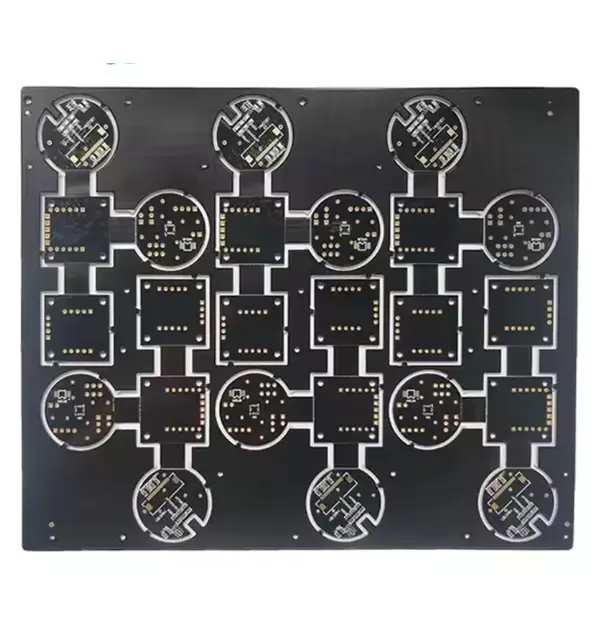
A successful PCB assembly for a power regulator begins with careful placement of each component. Engineers follow a systematic approach to ensure the circuit functions as intended. They start by organizing all parts, referencing the schematic and bill of materials. This preparation prevents confusion during assembly.
The step-by-step process for placing components on the PCB includes:
1. Organizing Components: Engineers switch to 2D layout mode in their design software. They use the Arrange Components tool to spread out parts for easier access.
2 . Moving and Rotating Components: They click and drag each component to its designated spot onthe PCBb. The SPACE bar rotates components in 90-degree increments, helping align them with the circuit flow.
3. Designator and Silkscreen Adjustment: Engineers move designators to readable positions. They make sure these labels do not overlap with pads or traces, which keeps the assembly process clear.
4 . Final Component Arrangement: The LM7805 voltage regulator sits centrally on the board. Input capacitors are placed close to the regulator’s input pin, while output capacitors are positioned near the output pin. This arrangement supports stable voltage regulation and reduces noise in the power supply.
Manual PCB etching sometimes comes into play for prototypes or small runs. In these cases, engineers transfer the circuit layout onto a copper-clad board, then use chemicals to remove unwanted copper. After etching, they drill holes for through-hole components and clean the board before starting assembly.
Soldering Methods
Engineers use two main soldering methods during PCB assembly for power regulator circuits: through-hole and surface mount. Each method offers unique advantages and challenges.
Through-Hole
Through-hole soldering remains popular for power supply circuits that require strong mechanical connections. Engineers insert component leads through holes in the PCB and solder them on the opposite side. This method provides:
●Strong thermal connections, which help with heat dissipation in voltage regulator circuits.
●High durability, allowing the assembly to withstand over 1,000 temperature cycles.
●Superior mechanical strength, making it ideal for environments with vibration or physical stress.
However, through-hole assembly can take more time and may not suit miniaturized designs. Engineers often choose this method for power regulators that handle higher currents or require robust connections.
Surface Mount
Surface mount technology (SMT) has transformed PCB assembly for power regulator circuits. Engineers place components directly onto the surface of the PCB, which allows for smaller and lighter designs. SMT offers several advantages:
| Advantage | Description |
|---|
| Miniaturization | SMT components are much smaller, reducing size and weight by up to 90%. |
| High Signal Transmission Speed | Compact structure and short circuit paths enable faster signal transmission. |
| Good High Frequency Effects | Lower RF interference due to reduced distributed parameters. |
| Automatic Production | High automation improves yield and reduces component failure. |
| Low Materials Cost | SMT components have lower packaging costs. |
| Simplified Production Process | Shorter process improves efficiency and reduces costs by 30%-50%. |
Despite these benefits, SMT also presents challenges:
| Disadvantage | Description |
|---|
| Power Limitations | SMT components usually handle lower power levels. |
| Fragility | Smaller parts are more prone to damage. |
| Soldering Complexity | High technical requirements can cause issues like tombstoning. |
| Inspection Difficulty | Visual inspection is harder due to miniaturization. |
| Equipment Investment | High initial investment in equipment is needed. |
Engineers select the soldering method based on the circuit’s requirements, the type of voltage regulator, and the intended application of the power supply.
Assembly Inspection
Inspection forms a critical part of PCB assembly for power regulator projects. Engineers use several techniques to ensure the circuit operates safely and reliably.
●Visual Inspection: Trained inspectors examine the PCB for defects. They look for burnt areas, discoloration, or loose components. They check for cracked solder joints, missing parts, and signs of damage on capacitors, such as bulging or leakage.
●Automated Optical Inspection (AOI): Machines scan the PCB to verify component placement and soldering quality. AOI reduces the risk of assembly defects in power supply circuits.
●X-ray Inspection: This method reveals hidden defects, such as soldering issues or short circuits beneath components.
●In-Circuit Testing (ICT): Engineers test the integrity and function of each component in the circuit. ICT identifies discrepancies and ensures the voltage regulator and other parts work as expected.
●Flying Probe Testing: This non-invasive method checks connectivity and function without custom fixtures. It suits low to medium volume production.
●Boundary Scan Testing: Engineers use this technique for digital components, especially in complex power supply circuits with built-in scan cells.
A well-executed PCB assembly for power regulator projects combines careful component placement, the right soldering method, and detailed inspection. This approach guarantees that the circuit meets performance and safety standards, supporting reliable operation in any application.
Testing and Troubleshooting Circuit
Initial Checks
Engineers begin the testing process with a series of initial checks to ensure the power supply circuit is safe and ready for operation. These steps help prevent damage to components and provide early verification of assembly quality.
1. They perform a thorough visual inspection of the assembled circuit. This step helps identify misplaced or missing components, solder bridges, and debris that could cause shorts.
2 . They use a multimeter to check the resistance between each power rail and ground. The resistance should not be near zero ohms, which would indicate a short circuit.
3.They confirm that no solder bridges or conductive debris exist on the board. Even a small piece of solder can compromise circuit stability.
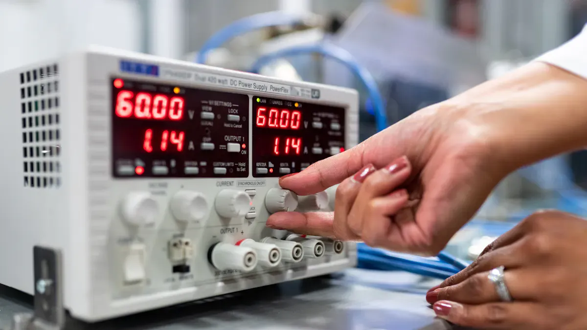
4.They apply power using a current-limited bench supply. This precaution limits the risk of damage if a fault exists in the circuit.
5. They monitor the current draw during power-up. An unexpectedly high current signals a possible short or incorrect component placement.
Output Measurement
After completing initial checks, engineers proceed to output the measurement. This phase focuses on verifying the voltage regulation and stability of the power supply circuit.
1. They use a voltmeter to measure the voltage across the regulator’s output terminals. Accurate voltage readings confirm that the regulator functions as intended.
2 . An oscilloscope allows them to observe the waveform of the output voltage. This instrument reveals any ripple or noise that could affect circuit stability.
3.For more precise verification, engineers use a high-resolution digital multimeter or a data logging system. These tools provide continuous monitoring and help detect subtle changes in voltage over time.
4.The oscilloscope also measures AC ripple on the power supply output. Excessive ripple indicates issues with filtering or regulator performance.
Engineers record all voltage measurements and compare them with the expected values from the schematic. Consistent results demonstrate proper operation and stability. Any deviation prompts further investigation before moving to advanced testing.
Load Testing
Load testing evaluates the stability and reliability of the power supply circuit under real-world conditions. Engineers simulate different load scenarios to observe how the regulator responds to changes in current demand.
●They connect a programmable load or a transient load generator to the output of the circuit. This equipment allows them to step the load current from zero to the maximum rated value and back.
●An oscilloscope monitors the output voltage during these load changes. Engineers look for voltage dips, overshoots, or oscillations that could signal instability.
●Current monitoring probes provide real-time data on how the circuit handles varying loads. These probes help verify that the regulator maintains voltage stability throughout the test.
●Engineers perform additional small load steps to evaluate fine stability characteristics. They observe the voltage response to each change, noting any signs of poor damping or slow recovery.
●They repeat the testing process at different input voltages and ambient temperatures. This comprehensive approach ensures the power supply remains stable under all expected operating conditions.
| Test Step | Purpose | Instrument Used |
|---|
| Step load from 0A to max | Check voltage stability and response | Oscilloscope, load gen |
| Small load steps | Evaluate fine stability and damping | Oscilloscope |
| Vary the input voltage | Confirm the regulator performance range | Bench supply |
| Monitor current | Ensure safe operation and circuit stability | Current probe |
Testing and troubleshooting form the backbone of power supply circuit verification. Careful measurement and observation at each stage ensure that the regulator delivers consistent voltage and maintains stability under all conditions.
Common Issues
Engineers often encounter several recurring problems during the testing phase of power regulator circuits. Recognizing these issues early helps maintain circuit reliability and safety.
●Unstable or Fluctuating Output Voltage
The output voltage may drift or oscillate instead of remaining steady. This instability can result from poor solder joints, incorrect component values, or faulty capacitors. Engineers use an oscilloscope to check the output waveform. A healthy regulator produces a clean, stable line. Any distortion or fluctuation signals a problem that requires further investigation.
●Overheating
Components such as the voltage regulator or nearby capacitors may become excessively hot. Overheating often points to excessive current draw, inadequate heat sinking, or a short circuit. Engineers check for proper heatsink installation and verify that the load does not exceed the regulator’s rating.
●Unusual Noises or Odors
Buzzing, hissing, or clicking sounds, as well as burnt smells, usually indicate electrical stress or component failure. These symptoms may arise from oscillations, overloaded components, or reversed polarity. Engineers immediately disconnect power and inspect the board for visible damage.
●Reduced Efficiency or Performance
The circuit may deliver less power than expected or operate inefficiently. This issue can stem from high resistance in traces, poor soldering, or degraded components. Engineers measure input and output power to calculate efficiency and identify losses.
The table below summarizes common symptoms and their possible causes:
| Symptom | Possible Cause | Diagnostic Tool |
|---|
| Fluctuating output voltage | Faulty capacitor, poor solder joint | Oscilloscope, multimeter |
| Overheating regulator | Excessive load, poor heatsink | Infrared thermometer |
| Unusual noise or odor | Component failure, reversed polarity | Visual, auditory check |
| Low efficiency | High resistance, degraded component | Multimeter, wattmeter |
Engineers address these issues by following a structured troubleshooting process. They inspect the board visually, measure voltages at key points, and use testing fixtures when necessary. Careful documentation of each step ensures that future troubleshooting becomes easier and more effective.
Documentation and Final Review
Assembly Records
Accurate assembly records help engineers track every detail of the PCB assembly process. These records support troubleshooting, future upgrades, and quality control. Each record should include the following information:
1. Reference Designator: Assign a unique identifier to each component, such as R1 for a resistor or C2 for a capacitor.
2.Part Number: Record the manufacturer’s part number to simplify sourcing and replacement.
3.Description: Add a brief note about the component, for example, "10kΩ Resistor, 0603 Package."
4.Quantity: List how many times each component appears on the board.
5.Package Type: Specify the physical size and shape, such as 0402 or 0805.
6.Manufacturer: Note the company that produces the component, if available.
7.Notes: Include extra details like tolerance, voltage rating, or special handling instructions.
Test Results
Documenting test results provides traceability and supports quality control. Engineers use a structured approach to record every step of the testing process. The table below outlines the key elements:
| Step | Description |
|---|
| 1 | Maintain comprehensive documentation and traceability throughout the process. |
| 2 | Record material certifications, inspection reports, test data, and rework logs. |
| 3 | Assign unique serial numbers to each board or batch for traceability. |
| 4 | Store records in a centralized system for easy access during audits or customer inquiries. |
Traceability allows engineers to identify issues quickly. They can narrow investigations to specific batches or components, which saves time and resources. A robust traceability system also prevents unnecessary recalls and protects the reputation of the brand.
Cost and Reliability
Several factors influence the cost and reliability of a power regulator PCB assembly project. Engineers must balance these factors to achieve a dependable and affordable design. The table below summarizes the main considerations:
| Factor | Description |
|---|
| Component Selection | Choosing standard packaging reduces assembly costs and improves reliability. |
| Sourcing Strategies | Bulk purchasing lowers costs but can tie up capital; rare components may increase expenses. |
| Manufacturing Complexity | Manual handling increases labor costs and assembly complexity. |
| Design Considerations | Electrical characteristics must match design requirements for reliable operation. |
Engineers who select standard components and plan sourcing strategies carefully can reduce costs. They also improve reliability by matching design requirements with the right electrical characteristics. Simple manufacturing processes lower labor costs and minimize errors.
This tutorial guides readers through each stage of PCB assembly for power regulators. Key steps include:
1.Prepare all materials and components.
2.Install components with correct orientation.
3.Apply solder and secure parts.
4.Inspect for defects and alignment.
5.Test the finished circuit for reliability.
Readers can use these steps to build power regulator circuits for many electronic projects. The tutorial highlights the value of proper component selection and layout. Sharing experiences or questions in the community helps everyone improve their skills.
About the auther:

Sonic Yang
As a major of Electronics and Mechanical Automation, Sonic has been engaged in PCB design, R&D, manufacturing of eletronics for around 22 years, as engineering director and coordinates with supply chain(components&CNC parts), providing professional supports and consults for global customers.
 en
en

.jpg)
 WhatsApp