Press-fit Process of Connectors on PCB&PCBA: Advantages and Limitations
I. Introduction to Press-fit Process
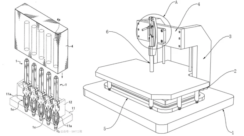
Press-fit is a technique that applies precise physical pressure to create a permanent, hermetically sealed mechanical and electrical connection between a connector (usually the connector's metal terminals) and a metallized hole on PCB&PCBA. It is solder-free, heating-free, a "cold soldering" process.
Core Process Steps:
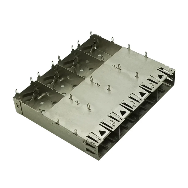
1. Preparation: Insert the connector with press-fit leads (such as crimp headers, D-Sub connectors, and some board-to-board connectors) into the corresponding through-holes on the PCB.
2. Positioning: Precisely position the PCB and connector assembly in the fixture of the pressing device such as positioning fixture.
3. Fit-pressing: The pressing punch (usually a dedicated pressing module) applies a preset pressure downwards. The punch's shape is designed to deform the pressing area of the terminals (usually a flexible "fisheye" shape or a slotted cylindrical shape).
4. Forming: Under pressure, the metal leads of the terminal undergoing plastic deformation, tightly filling the entire metallized hole on the PCB and potentially creating a slight engagement with the hole wall. Simultaneously, it eliminates air within the hole, forming a metal-to-metal connection.
5. Completion: After pressure released, due to elastic recovery, the terminal maintains a high-strength, durable connection with the hole wall, forming a reliable electrical path and mechanical fixation.
II. Key Advantages of Press-fit Process
1. High Reliability and Consistency:
● Eliminates soldering-related defects such as cold solder joints, bridging, solder spatter, and PCB thermal stress damage.
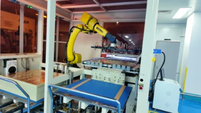
● Results are highly dependent on the precision of the pressing equipment and fixture(or molds), once parameters are set correctly, near 100% consistency can be achieved, suitable for automated mass production.
2. Heat-Free Process:
● Friendly to heat-sensitive components: No thermal damage to previously installed, heat-sensitive components (such as sensors and LEDs) or the PCB itself during high-temperature reflow soldering.
● Friendly to connectors which are not heat-resistant: Connectors with lower melting points or internal plastic components can be installed on PCB&PCBA with no potential risks.
● No thermal stress: Avoids thermal stress during solder joint cooling, which is especially important for high-reliability applications in military, aerospace, and automotive electronics.
3. Environmental-friendly and Simplify process:
● Eliminates the application of solder and flux, reducing the use of metals such as tin and lead, lowering BOM costs, and environmental-friendly(Lead-Free).
● No cleaning Process: Avoids potential corrosion risks from flux residue and cleaning process.
4. Potential flexibility of sequent process:
● Available to performed as the final step in the assembly process, preventing the connector from being exposed to high temperatures during subsequent reflow soldering.
● Easy to rework and repair: Using a dedicated pin removal tool, terminals can be removed from the holes (much more easier than desoldering), allowing replacement of individual pins or the entire connector with minimal PCB damage.
5. Excellent electrical and mechanical properties:
● The formed hermetic connection could prevent the intrusion of moisture and corrosive gases.
● The tight connection between metals could provide low and stable contact resistance.
● Resistance for mechanical vibration and fatigue: generally superior to solder joints, especially in environments with frequent insertion/removal or high vibration.
III. Limitations of Press-fit Process
1. Higher Upfront Costs and Design Constraints:
● Dedicated Connectors: Connectors with pressing-fit pins are generally expensive than soldering pin.
● Pressing Device and Fixtures: Initial investment for high-precision pressing device and fixtures.
● Strict Requirements for PCB Design: Extremely strict requirements for the diameter, copper thickness, and tolerances of PCB metallized holes. The hole diameter must perfectly match the size of the pins, with very tiny tolerances.
2. Process Irreversibility and Verification Difficulties:
● Invisible Process: After pressing, the connection quality cannot be easily inspected by visual or X-ray, not like solder joints which could be checked by internal filling of solder. Quality control relies on process monitoring.
● Difficult to repair once pressed: If pressing fails (e.g., pin or PCB hole damage), it is more difficult to repair than soldering and may need to replace the entire connector.
3. Higher requirements for mechanical stress:
● The pressing process causes mechanical impact on the PCB itself, requiring sufficient mechanical strength and lamination quality, otherwise, hole walls might be cracked.
● The retaining force between the connector and the PCB, which depends on the deformation and friction of the hole. For connection points to extremely high lateral tensile forces, additional mechanical fixation (such as clips or screws) may be required.
4. Limited scope of application:
● Not suitable for all connectors: Press-fit is difficult to design and implement for very miniaturized connectors or those with extremely small pin pitch.
5. Extremely sensitive to process parameters:
● Pressing quality is highly dependent on pressure, punch displacement, and alignment accuracy. Even slight deviations in these parameters could lead to poor connections or damage. Strict process verification and have to perform maintenance and calibration for both device&fixture.
IV. Summary and Application Scenarios
Pressing-fit is an important supplement and alternative for welding, it's core value lying on high reliability, heat-free process, and high consistency.
Typical Applications:
● Automotive Electronics: Engine control units, airbag modules (high vibration, high temperature cycling).
● Aerospace and Defense: Flight control systems, radar (extremely high reliability requirements).
● Industrial Equipment: PLC controllers, frequency converters (harsh environments, long lifespan).
● Communication Infrastructure: Base stations, routers (long-term stable operation required).
● High-Reliability Consumer Electronics: Servers, data storage devices.
A comprehensive trade-off is necessary to consider before going through pressing-fit process: If the electronic products have extremely high requirements for reliability, mass production volume, higher upfront costs is affordable and capable for strict process control, then pressing-fit is an ideal choice. Conversely, for cost-sensitive, design-variable, small-batch electronic products, traditional welding processes are usually more economical, flexible and also reliable.
Benlida is a professional electronics manufacturer for PCB and PCBA, for over 14 years, Benlida keeps invest on advanced equipment, with an experienced engineering team, committed to providing top-class EMS service to global customers! If your PCB&PCBA requires pressing-fit process, please feel free to contact Benlida for further details!
About the auther:

Sonic Yang
As a major of Electronics and Mechanical Automation, Sonic has been engaged in PCB design, R&D, manufacturing of eletronics for around 22 years, as engineering director and coordinates with supply chain(components&CNC parts), providing professional supports and consults for global customers.

 en
en



 WhatsApp