Temperature and pressure control stand at the core of the Multi-layer PCB lamination process. BenPCB’s advanced lamination ensures precise layer bonding, which supports high density, reliability, and superior performance in complex electronic systems. Without careful regulation, defects such as delamination, warping, or electrical failures may occur. Manufacturers who understand the practical impact of these parameters can achieve better product quality and long-term functionality.
Multi-layer PCB Lamination Process Overview
Layer Stacking and Preparation
The multi-layer pcb lamination process begins with careful layer stacking and preparation. Engineers select core boards with etched circuit patterns. These cores are stacked with sheets of prepreg, which is a resin-coated fiberglass material. The order of stacking is important because it determines how signals and power will flow through the board. Each layer must align perfectly to avoid electrical problems later.
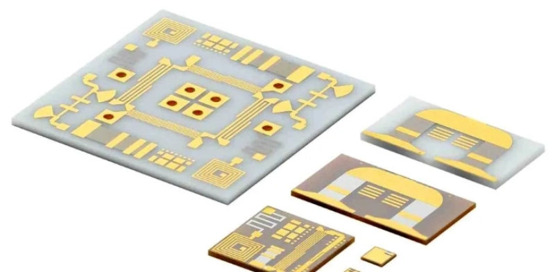
BenPCB’s multi-layer pcb uses advanced stacking techniques. This allows for high-density layouts and supports complex applications like AI servers and medical devices. The stacking process also helps separate signal layers from power and ground planes. This reduces interference and improves signal quality.
The main steps in the process can be summarized as follows:
| Step | Description |
|---|
| Lay-up | Stacking and fixing core boards with etched circuit patterns and prepreg in a specific order. |
| Lamination | Clamping the inner layers and applying heat and pressure to bond them together. |
| Post-treatment | Processing the boards through bevelling, drilling, and checking for layer deviations. |
Application of Temperature and Pressure
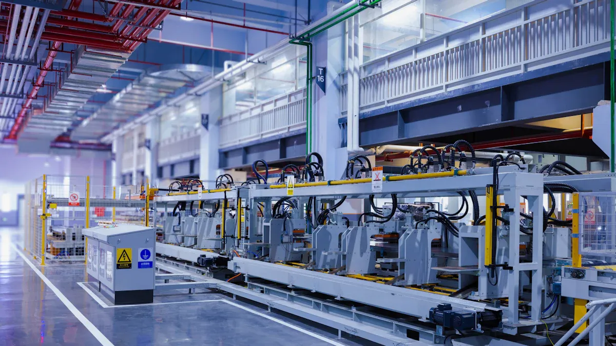
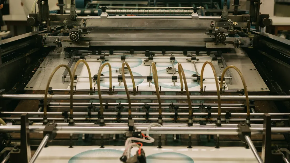
After stacking, the lamination process moves to the application of temperature and pressure. The stacked layers are placed in a vacuum heat press. The press applies controlled heat and pressure to the stack. This causes the resin in the prepreg to flow and fill any gaps between layers. The heat also cures the resin, creating a solid bond.
Precise control of temperature and pressure is essential. If the temperature is too low, the resin may not flow properly. If the pressure is too high or too low, layers can shift or form voids. BenPCB uses advanced equipment to monitor these parameters. This ensures strong adhesion and reliable performance in every board.
Temperature Effects in Lamination
Resin Flow and Curing
Temperature plays a crucial role in the multi-layer pcb lamination process. The resin in the prepreg must flow and cure properly to bond the layers together. When the temperature rises, the resin viscosity drops, which allows it to move and fill gaps between layers. If the temperature is too low, the resin becomes thick and may not spread evenly. This can leave voids and weak spots in the pcb.
●Higher temperatures reduce resin viscosity, enhancing flow.
●Lower temperatures increase viscosity, risking incomplete filling.
●The optimal lamination temperature for FR-4 is between 180°C and 190°C.
●High-Tg materials may require temperatures around 200°C for complete curing.
●Controlled temperature ramp rates are essential to prevent defects like voids and delamination.
The lamination process follows a careful sequence:
- Preheat the stack-up to 100°C–120°C before applying full pressure to initiate resin flow.
- Gradually apply pressure in sync with temperature increases to avoid excessive resin expulsion.
- Maintain stable curing temperatures for 60 to 120 minutes to ensure proper cross-linking.
Tip: The hot plate temperature in lamination presses is typically kept between 180°C and 200°C. This range allows the epoxy resin to soften and flow effectively before curing.
Impact on Layer Integrity
Temperature variations during the multi-layer pcb lamination process can affect the integrity of each layer. If the temperature fluctuates, air bubbles may form and pressure may become uneven. These issues can harm the dielectric properties and bonding strength of the pcb. Precise control of temperature is necessary to keep the layers stable and reliable.
Thermal stress testing methods, such as thermal cycling and thermal shock, help evaluate how well a pcb can handle temperature changes. These tests simulate real-world conditions and reveal weaknesses in the design or materials. As devices become more compact, thermal challenges increase. Testing methods like reflow simulation, thermal cycling, and thermal shock are crucial for assessing a pcb's ability to withstand temperature variations without delamination or warpage.
Risks of Incorrect Temperature
Incorrect temperature during lamination can cause several defects in the pcb. If the temperature is too high, the resin may flow too much or even decompose, which weakens the bond. If the temperature is too low, the resin will not melt enough, preventing a strong bond.
| Cause | Description | Resulting Risk |
|---|
| Improper press profile | Incorrect temperature or pressure | Incomplete curing |
Common risks include:
●Excessive resin flow leading to thin bonding layers.
●Resin decomposition causing weak adhesion.
●Incomplete melting resulting in poor bonding.
●Formation of voids and delamination.
Careful monitoring and control of temperature throughout the multi-layer pcb lamination process help prevent these defects and ensure the pcb meets high standards for density and reliability.
Pressure Effects in Lamination
Layer Bonding and Adhesion
Pressure plays a vital role in the multi-layer pcb lamination process. When engineers apply the right amount of pressure, the resin flows between the layers and fills every microgap. This action creates strong bonds that hold the layers together. If the pressure is too low, the resin cannot reach all the spaces, and the layers may not stick well. If the pressure is too high, the resin can break down, which weakens the bond.
The following table shows how different pressure levels affect layer bonding:
| Pressure (PSI) | Effect on Layer Bonding |
|---|
| 250 - 400 | Optimal resin flow and strong interlayer bonds |
| Below 250 | Weak bonds and potential defects |
| Above 400 | Risk of resin degradation and voids |
Most manufacturers use a pressure range between 300 and 500 psi to achieve reliable adhesion. This range helps the resin fill all the tiny gaps and ensures that each pcb layer bonds tightly. Controlled pressure also reduces the risk of delamination, which can cause failures in electronic devices.
Note: The application of controlled pressure during lamination is crucial for ensuring that the resin adequately fills the microgaps between the layers of a pcb. This filling is essential for achieving strong adhesion and preventing issues such as delamination, which can compromise the integrity of the final product.
Void Elimination
Voids are small air pockets that can form between layers during the lamination process. These voids can weaken the pcb and cause electrical problems. Proper pressure helps eliminate these voids by pushing the resin into every space between the layers. When the resin fills all the gaps, the layers become one solid unit.
Key points about void elimination:
●Controlled pressure (200–300 psi) is essential for proper adhesion.
●Pressure ensures resin fills microgaps between layers effectively.
●Proper pressure minimizes defects such as voids and delamination.
A pcb with no voids will have better electrical performance and last longer. BenPCB uses advanced equipment to monitor and control pressure during lamination. This approach helps produce high-quality boards for demanding applications.
Risks of Incorrect Pressure
Incorrect pressure during the multi-layer pcb lamination process can lead to several problems. If the pressure is too low, the resin does not flow well, and the layers may not bond. This can cause weak spots or even separation between layers. If the pressure is too high, the resin may break down or get squeezed out, leaving gaps or creating voids.
Common risks include:
●Weak layer bonding, which can lead to delamination.
●Formation of voids that reduce electrical reliability.
●Resin degradation, which weakens the pcb structure.
Careful control of pressure is necessary to avoid these risks. Engineers must monitor the process closely to ensure each pcb meets strict quality standards. Reliable pressure control supports the long-term performance and durability of every board.
Optimal Ranges and Quality Control
Recommended Temperature and Pressure
Selecting the right temperature and pressure is essential for a successful multi-layer pcb lamination process. Industry guidelines recommend the following ranges for common materials:
●Temperature for FR-4 materials: 180°C to 200°C (356°F to 392°F)
●Pressure for standard multilayer boards: 250–350 psi
●Pressure for high-layer-count boards: 300–400 psi
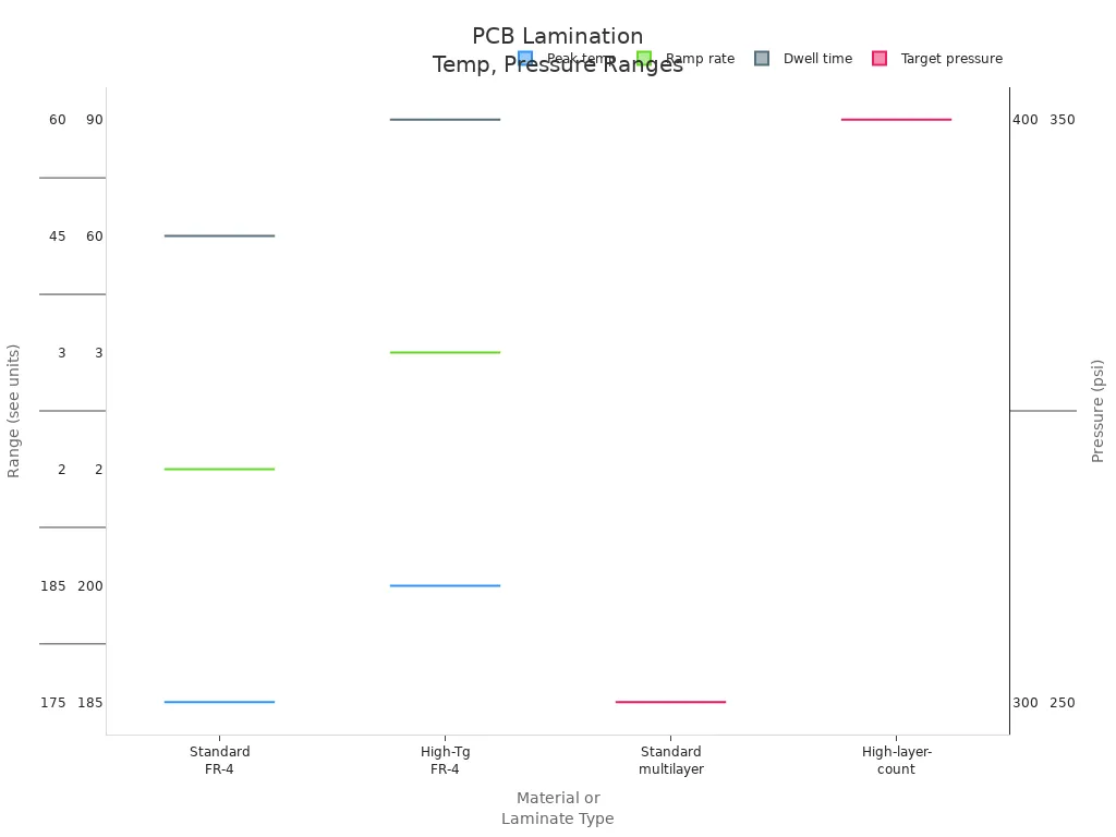
International standards, such as IPC-6012, provide more detailed targets for different materials. The table below summarizes these values:
| Parameter | Standard FR-4 | High-Tg FR-4 | Polyimide | Rogers |
|---|
| Peak temp | 175-185°C | 185-200°C | 200-220°C | 190-210°C |
| Ramp rate | 2-3°C/min | 2-3°C/min | 1.5-2°C/min | 2-3°C/min |
| Dwell time | 45-60 min | 60-90 min | 90-120 min | 60-90 min |
Target pressures:
●Standard multilayer: 250-350 psi
●High-layer-count: 300-400 psi
●PTFE materials: 100-200 psi
●Heavy copper (3+ oz): 350-400 psi
Vacuum level: Less than 5 mbar (0.5 kPa) before heat application.
Consequences of Deviations
Maintaining specific temperature and pressure settings during the pressing process is crucial for the quality of multi-layer PCBs. Deviations from the recommended ranges can lead to significant issues such as delamination, warping, and weak copper bonds. These problems compromise the integrity and reliability of the boards. Even small changes in process parameters can result in defects that affect the electrical and mechanical performance of the pcb.
Note: Consistent control of temperature and pressure helps prevent costly failures and ensures each pcb meets strict industry standards.
Common Defects
When temperature or pressure falls outside the optimal range, several defects may appear in the pcb:
●Delamination between layers
●Voids or air pockets inside the board
●Warping or bending of the finished pcb
●Weak copper-to-resin bonds
●Incomplete resin curing
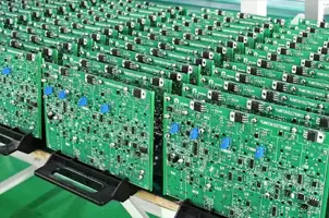
These defects can reduce the lifespan of the pcb and cause failures in demanding applications. Careful monitoring and quality control during lamination help BenPCB deliver reliable boards for advanced electronics.
Practical Challenges and Solutions
Monitoring and Control Methods
Manufacturers face several challenges when controlling temperature and pressure during the pcb lamination process. Uneven temperature profiles can cause delamination or warpage. Inconsistent pressure may lead to voids between layers. Advanced monitoring technologies help address these issues. Multi-zone heating systems maintain temperature uniformity within ±2°C across the platen. Modern lamination presses use precise sensors to track both temperature and pressure in real time. These systems allow operators to adjust parameters quickly, reducing the risk of defects in the pcb.
| Method | Benefit |
|---|
| Vacuum-assisted lamination | Reduces internal defects |
| Optimized temperature ramp | Ensures consistent curing |
| Controlled pressure distribution | Improves interlayer bonding |
| Multi-stage curing processes | Enhances overall yield and quality of PCBs |
BenPCB uses these advanced methods to ensure every pcb meets strict quality standards.
Equipment Variability
Equipment variability can impact the consistency of the pcb lamination process. Multi-zone vacuum lamination presses control temperature and pressure across different zones. This approach ensures even curing and reduces internal stress. However, even small differences in equipment calibration can affect the final product. Proper calibration prevents uneven heating and thermal shock. It also helps adjust for changes in material batches. BenPCB invests in modern equipment and regular calibration to maintain high reliability.
Ensuring Consistent Results
Manufacturers follow best practices to achieve consistent results in pcb production. Calibrated presses with multiple zones ensure uniform pressure and temperature. Cooling under full pressure to 50°C locks in flatness. Witness coupons track actual process conditions, allowing for immediate adjustments. Operators record lamination parameters for each run, building a database for troubleshooting. Post-lamination inspections, such as X-ray and cross-sectional analysis, verify the structural integrity of each pcb. BenPCB’s commitment to these practices supports long-term performance and reliability.
Precise control of temperature and pressure is essential for producing high-quality pcb boards. These parameters enhance bonding strength, reduce defects, and ensure long-term reliability. BenPCB’s advanced lamination methods support consistent pcb performance by minimizing voids and maintaining layer integrity. Even small temperature changes can affect resin flow and pcb quality.
Engineers and manufacturers should focus on:
●Monitoring pcb lamination temperature and pressure
●Using new materials and proper storage
●Ensuring even heat and pressure during curing
●Aligning layers carefully for each pcb
 en
en

 WhatsApp