Home > Blog > Industry News > Advanced HDI PCB Solutions: Emerging Technologies and Their Impact on Electronic Product Development
Advanced HDI PCB Solutions: Emerging Technologies and Their Impact on Electronic Product Development
Share
Dec 26
Source:
You see advanced HDI PCB solutions changing electronics today. Benlida Circuit uses new ideas to improve technology. Smaller devices need more power and work faster. HDI means high-density interconnect. It helps fit many parts in small spaces. This process helps make products like smartphones and medical sensors smaller. The HDI PCB market was about USD 9.6 billion in 2023. It may grow to USD 17.3 billion by 2032. The main reasons are the need for small, strong electronics. New technology brings big changes and new chances.
The HDI PCB market was worth USD 9.6 billion in 2023.
Experts think it could be USD 17.3 billion by 2032.
The market grows because people want smaller and better devices.
Key Takeaways
HDI PCBs let more parts fit on a board. This helps make devices smaller. These devices can also do more things.
Microvias and ultra-fine traces help signals stay strong. This means data moves faster. There is less loss of signal.
Using HDI technology can lower costs to make things. Designs can be simpler. Fewer layers are needed.
Advanced materials like low-Dk substrates make electricity work better. They also help stop electromagnetic interference.
Embedded passives in HDI boards give cleaner power. Devices use less power. This helps batteries last longer.
The HDI PCB market is growing fast. People want smaller and smarter electronics. Many industries need these products.
HDI technology helps build high-performance devices for 5G and AI. These devices have faster and better connections.
Picking HDI PCBs helps companies launch products faster. Design changes are quick. Manufacturing is more efficient.
HDI PCB Overview and Importance
What Is High-Density Interconnect
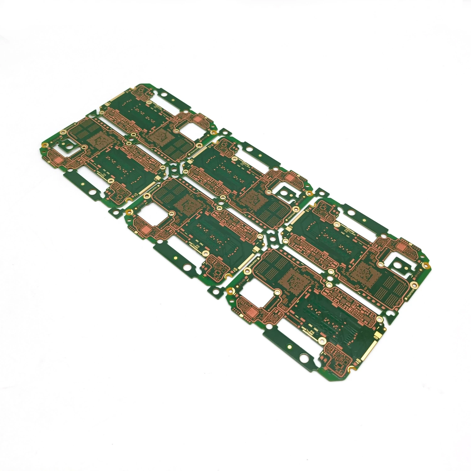
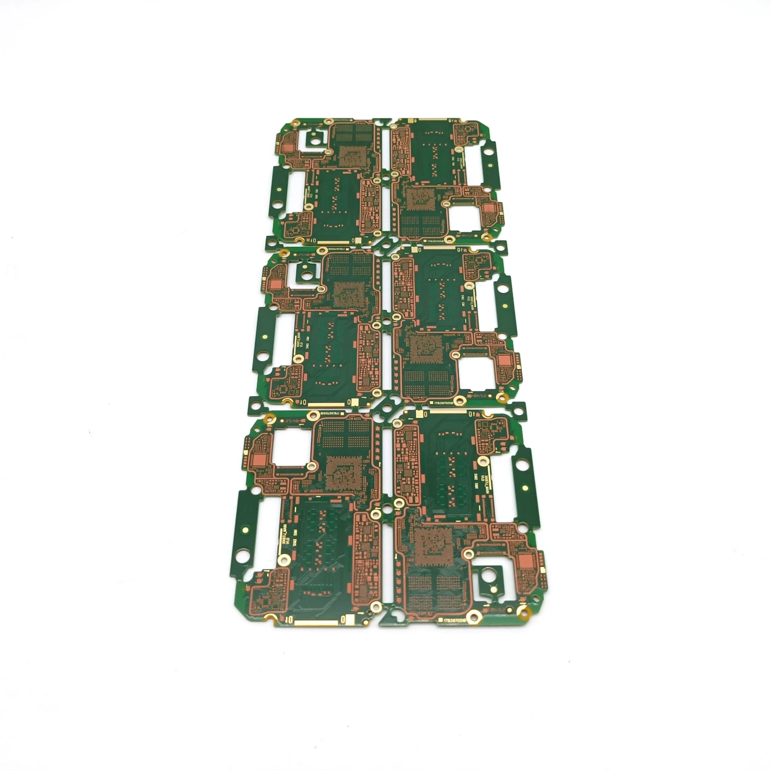
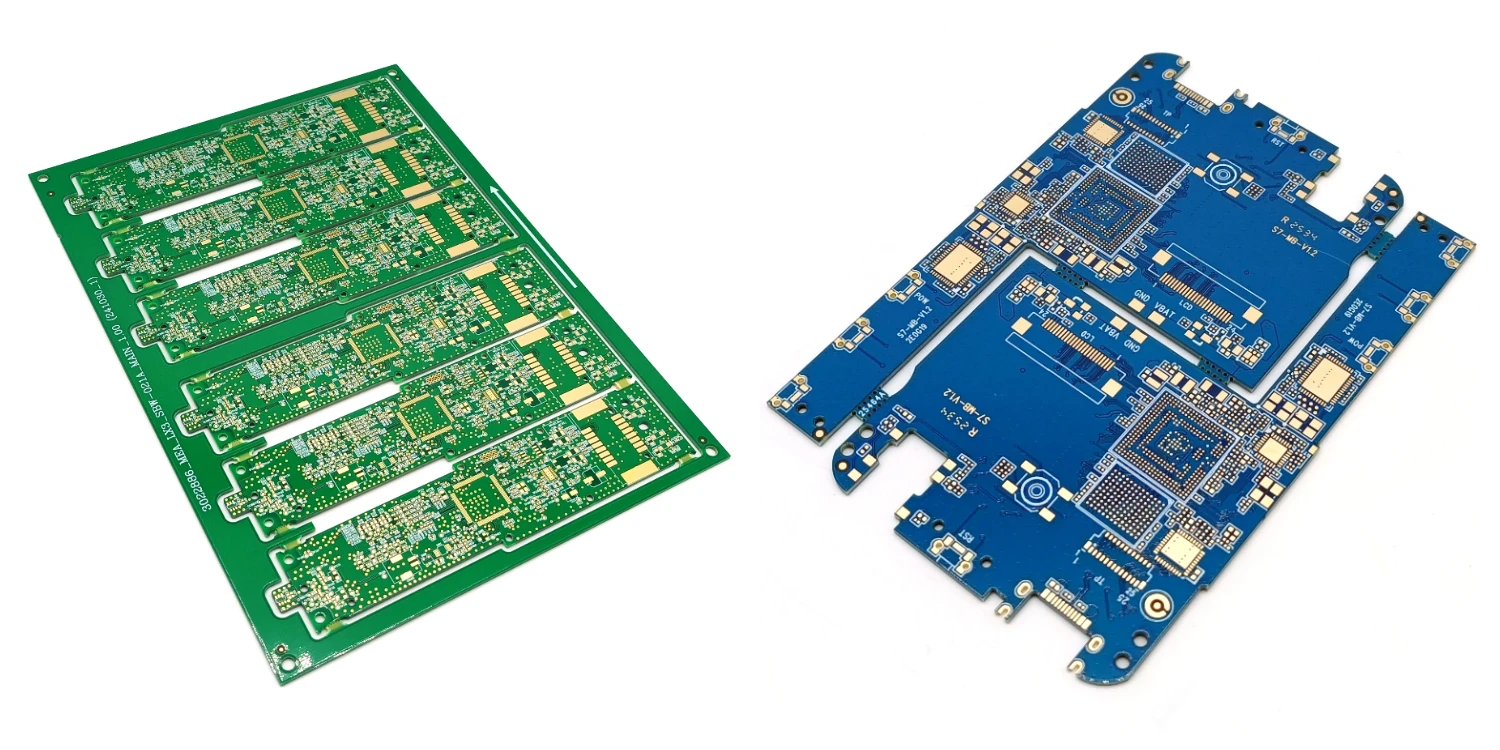
High-density interconnect is a big change in circuit board design. These printed circuit boards let you put more features in small spaces. You do not lose reliability when you use HDI. HDI boards have more wires packed close together than regular boards. They use thinner spaces and smaller vias. The connection pads are packed tightly. You find HDI technology in things like smartphones and medical devices. Micro-via technology helps make wiring even denser. If you want to make small products, HDI is a good choice.
HDI PCBs help you fit more features in less space.
You get thinner lines and smaller vias for better results.
Micro-via technology lets you make compact designs.
High density interconnect is used in modern electronics.
Key Features of HDI PCBs
HDI PCBs have special features that make them different from regular boards. The table below shows some main differences:
Feature
HDI PCBs
Traditional PCBs
Microvia Technology
Uses microvias for better connections
Does not use microvia technology
Layer Construction
Often has more than 8–16 layers
Usually has fewer layers
Electrical Performance
Has less stray capacitance and signal loss
Has more stray capacitance and signal problems
Application Suitability
Good for important applications
Not good for high-performance uses
Other features you see in HDI PCBs:
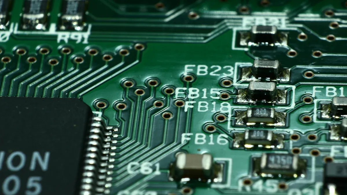
Finer lines and smaller vias help you get more connection pads.
Many layers with microvias allow advanced functions in small designs.
You use microvias, blind and buried vias, and very thin lines.
HDI boards often have more than 8–16 layers, so you have more ways to design.
Why HDI Matters in Electronics
High density interconnect is important for new electronics. It helps make devices smaller. HDI lets you put more parts on small circuit boards. This is needed for things like smartphones and wearables. HDI boards have better signal quality because the connections are packed closer. This helps with high-frequency uses in telecom. HDI also supports fast data transfer, which is needed for electronics and cars. When you pick HDI, your products get faster, smaller, and more reliable.
Tip: If you want to build small, powerful devices, HDI PCBs can help you do it.
Advanced HDI PCB Solutions and Technologies
Microvias and Ultra-Fine Traces
Miniaturization and Density
Miniaturization is very important in electronics today. Advanced hdi pcb solutions use microvias and ultra-fine traces. These help fit more parts into smaller spaces. You can design small devices like wearables and smartphones. Microvias are tiny holes that connect layers inside the pcb. Ultra-fine traces are thin lines that carry signals between parts. These features let you make boards with more parts but still work well.
Here is a table that shows why microvias and ultra-fine traces are helpful:
Advantage
Description
Miniaturization and Space Savings
Ultra-fine traces and microvias help designers fit more parts in a small area. This is important for small devices like wearables.
Superior Signal Integrity
Shorter signal paths in Ultra-HDI PCBs keep signals strong and help high-frequency uses like 5G and fast computers.
Enhanced Thermal Management
Special features like blind and buried vias help move heat away, so devices do not get too hot.
Increased Reliability and Durability
Stacked via technology makes strong connections that last a long time, even under tough conditions.
Electrical Performance Optimization
Shorter trace lengths use less power and help batteries last longer. Complex designs also spread power better and lower noise.
These new ideas help you build smaller and stronger products. Advanced hdi pcbs let you add more features in less space.
Signal Speed and Reliability
Microvias and ultra-fine traces do more than save space. They also make signals faster and more reliable. Microvias create shorter paths for signals. This means less signal loss and faster data. Ultra-fine traces lower unwanted effects like capacitance and inductance. This is important for fast and high-frequency designs. You also get less cross-talk and less electromagnetic interference. Your devices work better and more reliably.
Microvias make signal paths shorter, so signals stay strong and do not lose quality.
Smaller microvias lower capacitance and inductance, which helps with fast designs.
Good signal routing with microvias means less cross-talk and less electromagnetic interference.
With these new ideas, your pcb works well in many uses, from flexible circuits to high-performance pcbs.
Laser Drilling and Direct Imaging
Precision and Yield
Laser drilling and direct imaging are new ways to make hdi pcbs. Laser drilling uses light to make tiny, exact holes called microvias. Direct imaging uses lasers to draw patterns on the board. These methods help you make boards with high accuracy every time.
Here is a table that shows the good things about laser drilling and direct imaging:
Benefit
Description
Precision
Laser drilling makes very small microvias and puts holes in the right place.
Efficiency
Using both laser drilling and direct imaging helps meet strict rules and saves money.
Fine Feature Resolution
Laser direct imaging gives high accuracy for making dense patterns in HDI designs.
You get more good boards because these methods lower mistakes. This means you make more boards with fewer problems. You also save time and money when making boards. Laser drilling and direct imaging help you make advanced hdi pcb solutions for new devices.
Advanced Materials for HDI
Low-Dk Substrates
Picking the right materials is important for hdi pcb making. Advanced hdi pcb solutions use special materials called low-Dk substrates. Dk means dielectric constant. Low-Dk materials help you get better electrical performance and make boards easier. They are needed for fast designs and flexible circuits.
Here is a table of common advanced materials used in hdi pcb making:
Material
Properties
Applications
Polyimide
Flexible and strong, good for multilayer flex PCBs
Flexible electronics
BT-epoxy
Keeps out moisture and holds its shape
General HDI PCBs
ABF
Lets you make very thin lines and works with laser drilling
High-density interconnects
RCC
Costs less and handles heat well
Cost-sensitive applications
PTFE
Has a low dielectric constant and works with high-frequency signals up to 10 GHz
High-frequency applications
Low-Dk substrates let you use bigger conductor sections. This lowers losses at high frequencies. It is important for digital signals that move very fast. You get better signal quality and higher bandwidth.
Impedance Control and EMI Reduction
Low-Dk materials also help you control impedance and lower electromagnetic interference. When you use these materials, you can hit exact impedance goals. This is important for fast data and good signal transmission.
Low-Dk materials are needed for fast PCB designs. They help make boards better and work well.
Using low-Dk substrates helps you reach impedance goals by letting you use bigger conductor sections. This lowers losses at high speeds.
Lower dielectric constants lower mutual capacitance. This makes signals better and increases bandwidth.
Lower Dk values mean less mutual capacitance compared to self-capacitance. This helps control crosstalk.
Thinner dielectrics help control crosstalk by making self-capacitance higher for a given trace width and spacing.
Using wider traces with low-Dk materials lowers crosstalk problems compared to high-Dk materials.
You can see how these new ideas in materials and making help you build strong, fast, and efficient pcbs. Advanced hdi pcb solutions from Benlida Circuit use these new technologies to give you great results in every use, from flexible circuits to high-performance pcbs.
Embedded Passives and Power Efficiency
Embedded passives change how you design hdi boards. You do not need to put every resistor, capacitor, or inductor on top. You can build these parts inside the board layers. This makes your design smaller and helps your device work better.
Cleaner Power Delivery
You want your device to get steady power. Embedded passives help in many ways:
You can put resistors, capacitors, and inductors inside the hdi board. This saves space and keeps things tidy.
These built-in parts lower unwanted capacitance and inductance. Your signals stay strong, even when moving fast.
Embedded passives help control heat. They are inside the board, away from outside heat, so your device stays cooler.
When you use embedded passives, your device gets the power it needs. There is less noise and fewer drops. The table below shows how each passive part helps with power and keeps your device working well:
Component
Role in Power Delivery and Consumption
Resistors
Limit current and divide voltage, protecting parts from too much current.
Capacitors
Smooth out power changes, giving steady DC voltage.
Inductors
Filter high-frequency noise, making sure power stays clean.
Reduced Power Consumption
You want your device to last longer and use less energy. Embedded passives help you do this. When you put these parts inside the hdi board, signal paths get shorter. Shorter paths mean less power lost as heat. Your device can run cooler and use less battery.
You also get better results at high speeds. Embedded passives lower signal loss and keep circuits working fast. You can fit more parts in a smaller space, so you can build smaller and lighter devices.
Note: Using embedded passives in your hdi design gives you cleaner power and helps save energy. Your device works better and lasts longer.
HDI Benefits for Electronics Development
Miniaturization and Integration
People want devices to be small and smart. Advanced hdi pcb solutions help make this happen. HDI lets you put more parts in a tiny space. This is important for things like smartwatches and tablets. Microvias and fine-pitch parts make boards lighter and thinner. You can place parts very close together, less than 0.5 mm apart. This means you add more features without making the device bigger.
Microvias make pcb boards smaller and lighter, which is good for portable devices.
Microvias help signals travel shorter paths, so signal quality gets better. This is needed for fast things like 5G.
Fine-pitch parts let you fit more functions in small spaces.
Stacking layers gives you more ways to design. You can build boards with up to 20 layers in the same space as old boards.
You get more power and features in a small device. This new way helps you make electronics that are both small and strong.
Performance and Reliability
Devices need to be fast and last a long time. HDI technology gives better performance and reliability than old pcbs. You see more parts packed together and better signal quality. HDI can handle data speeds over 10 Gbps, which is great for new electronics. Shorter and layered connections mean less signal loss and less crosstalk.
Aspect
HDI PCBs
Conventional PCBs
Component Density
More parts in less space
Fewer parts, more space
Signal Integrity
Better signal quality, less loss
Normal signal quality
Performance in High-Speed
Works with data over 10 Gbps
Not as good for fast data
Reliability
Handles tough conditions
Not as strong in hard places
Crosstalk
Less crosstalk because parts are close
More crosstalk possible
EMI Reduction
Special materials and design lower EMI
Regular EMI control
Temperature Range
Works from -40°C to 85°C
Smaller temperature range
HDI pcbs lower signal loss and crosstalk. Shorter and layered paths make them good for telecom and computers. Strong materials and careful building help these boards handle heat and shaking. You can trust hdi boards in hard places, like planes or hospitals.
Tip: HDI boards help your electronics work well, even when things get tough.
Cost Optimization
People want to save money and get good results. HDI pcb technology helps with both. You can make designs simpler by using fewer layers, which saves money. Making the boards is faster and easier. Microvias and thin lines help boards work better in small spaces. This helps with heat and lowers signal loss. Your products last longer and work better, so you save money over time.
Picking the right materials is important. HDI pcbs use materials that meet safety and quality rules. You get more good boards and spend less fixing broken ones. Advanced hdi pcb solutions help you get better results and lower costs.
Note: Choosing hdi means you get new ideas, save money, and make your devices better.
Speed to Market
You want your new product to reach customers quickly. Using hdi technology helps you do this. When you use hdi PCBs, you can design smaller and more powerful devices. This means you can fit more features into a compact space. You do not have to wait for new materials or special parts. You can use hdi to solve design problems fast.
Here are some ways hdi PCBs help you speed up your product launch:
You can create complex layouts in small spaces. This lets you add more functions without making the device bigger.
You do not need to redesign your product for every new feature. hdi boards give you the flexibility to change layouts quickly.
You can test and update your designs faster. Shorter signal paths and better performance mean fewer problems during testing.
You can work with manufacturers who use advanced tools like laser drilling and direct imaging. These tools help you get high-quality boards in less time.
You do not have to worry about the limits of old PCB technology. hdi meets the needs of modern electronics, so you can move forward with your ideas.
Tip: When you use hdi PCBs, you can keep up with fast-changing markets. You can launch new products before your competitors.
You can see how hdi technology helps you stay ahead. You get more design options, faster testing, and quicker production. This means your product can reach the market sooner and make an impact.
Real-World Applications of HDI PCBs
Consumer Electronics
HDI technology is used in many electronics you know. Smartphones, tablets, and wearables all use HDI PCBs. A foldable smartphone has a rigid-flex HDI PCB. This lets the phone bend over 100,000 times. The traces do not break. Regular boards break after only 10,000 bends. Devices are lighter, thinner, and stronger because of HDI.
Here is a table that shows how HDI PCBs help different products:
Product Type
Advantages of HDI PCBs
Smartphones
Higher component density, reduced weight and size
Tablets
Improved electrical performance, enhanced signal integrity
Wearables
Miniaturization for complex systems in smaller footprints
Medical Devices
Capability for high-density connections in compact spaces
You get more parts in a small space. Devices work better and weigh less. Signals are clearer. Wearables like smartwatches use HDI PCBs. They fit many parts into small, comfy designs.
Medical Devices and Sensors
HDI PCBs are important in medical devices. CT and MRI machines use HDI boards for sensor arrays. These boards process fast signals. Pacemakers and neurostimulators use HDI PCBs. They need to be small and work well for years. This is important inside the body.
Patient monitors like glucose meters use HDI PCBs. They stay thin and easy to wear. You can put many sensors on small boards. Surgical robots and endoscopes use HDI PCBs too. These boards help control tools and send clear video in tight spaces.
HDI PCBs make medical devices smaller and stronger.
Devices work better for imaging, monitoring, and surgery.
Devices last longer because of good PCB design.
Automotive and Aerospace
HDI PCBs are used in cars and planes. In cars, they help with safety and driver systems. They make sure things work right. New cars need strong and safe PCBs.
In planes and space, HDI PCBs work in tough places. They handle heat and radiation. Satellites, drones, and missiles use HDI PCBs. These boards are small and reliable. They last a long time.
HDI PCBs keep cars and planes safe.
You can make small systems for vehicles and planes.
These boards work well even in hard conditions.
Note: HDI PCBs help with 5G and fast devices. Your devices get quicker and more reliable.
5G and AI Hardware
5G and artificial intelligence are changing how devices work. HDI PCBs help make these new technologies possible. They let devices handle faster data and smarter tasks.
5G networks move lots of data very quickly. HDI PCBs give high-speed paths for signals. This means less signal loss and better results. HDI boards are small, so you can fit more parts in tight spaces. This helps with 5G base stations, antennas, and mobile devices. You can build equipment that works faster and uses less power.
AI hardware needs to process lots of information at once. HDI technology lets you put more chips and sensors on one board. This helps AI devices think and react faster. You see this in smart cameras, voice assistants, and robots.
Here are ways HDI PCBs help with 5G and AI hardware:
HDI PCBs help send data fast for 5G networks.
You can fit more parts on smaller boards, which helps make devices tiny.
HDI technology makes it easier to build complex systems in small spaces.
You get better signals, which is important for fast and reliable connections.
Devices use less power because signal paths are shorter.
Benlida Circuit’s HDI PCBs have features that help these uses. You get microvias as small as 50μm and ultra-fine traces down to ≤40μm. These let you design boards with up to 10 times more parts than regular PCBs. Your 5G modules and AI processors can run fast with less than 0.2dB signal loss at 40GHz. You also get low-Dk materials like Rogers 4003C and Megtron 7. These help control impedance and lower electromagnetic interference.
Here is a table that shows how HDI PCBs help 5G and AI hardware:
Feature
Benefit for 5G and AI Hardware
High Component Density
More chips and sensors in smaller devices
Fast Signal Paths
Quicker data transfer and processing
Low Power Consumption
Longer battery life and cooler operation
EMI Reduction
Stable performance in noisy environments
Precision Engineering
Reliable operation at high frequencies
Tip: If you want your 5G or AI device to be faster, smaller, and smarter, HDI PCBs give you what you need.
You see HDI PCBs in 5G smartphones, smart home hubs, and AI wearables. These boards help devices connect, learn, and respond right away. When you pick advanced HDI solutions from Benlida Circuit, your products are ready for the world of 5G and AI.
Market Trends and Growth Drivers
HDI PCB Market Expansion
The hdi pcb market is getting bigger fast all over the world. Many companies want devices that are smaller and smarter. This makes them need better boards. In 2024, the market was worth USD 18.7 billion. Experts think it will grow by 10.2% every year from 2025 to 2033. By 2033, the market could be USD 48.5 billion. Asia Pacific will have the biggest share at 76.9% in 2025. The FR4 segment will be about 31.8% of the market. Smartphones and mobile devices will take up 29.3%. These numbers show that more people want new technology and better boards.
The global HDI PCB market was USD 18.7 billion in 2024.
It could reach USD 48.5 billion by 2033.
Asia Pacific will have 76.9% of the market in 2025.
The FR4 segment will be 31.8% in 2025.
Smartphones and mobile devices will be 29.3% in 2025.
Demand in 5G and IoT
You see more devices using 5g and IoT every day. These need boards that can handle fast signals and hard designs. People want higher bandwidth and less waiting time. This makes companies use better pcb technology. 5g needs to move data quickly and keep connections strong. IoT needs many devices to talk to each other right away. HDI pcbs help with fast digital designs and tricky signal paths. As 5g and IoT grow, hdi boards become very important for new networks and data centers.
More bandwidth means people want better boards.
Less waiting time is key for 5g and IoT.
New technology needs tricky signal paths.
More devices talking means strong pcb solutions are needed.
5g and IoT growth make companies use hdi pcbs.
Material and Manufacturing Innovations
You get help from new materials and better ways to make pcbs. Some substrates move heat well, over 3 W/mK, which helps with power and LED boards. Sequential build-up technology lets you make complex connections that work well. Microvia technology now makes tiny holes, only 50 micrometers wide, using lasers. Filled microvias use copper or paste to make boards work better and fit more parts. Low-loss dielectric materials like special polyimide and liquid crystal polymer help with fast 5g signals. Special products for 5g base stations and mobile devices need to work well at high speeds. New ways to make boards, like laser drilling and direct imaging, help with signal quality, strong boards, and small designs.
Tip: You can use these new ideas to make boards faster and stronger.
Innovation Type
Benefit for PCB Production and Applications
Thermally Conductive Substrates
Better heat control for power and LED boards
Sequential Build-Up Technology
Strong and complex connections
Microvia Technology
Smaller holes for more parts and better boards
Low-Loss Dielectric Materials
Better signals for 5g technology
Advanced Fabrication Techniques
Stronger boards and smaller designs
You can see how these changes help you make better boards for things like medical, 5g, and other new uses. Better ways to make boards and new materials help you work faster and make stronger technology.
Challenges and Future Outlook
Supply Chain and Manufacturing
Working with HDI technology brings many problems. People want smaller and stronger devices. This makes designs harder. You have to pick materials that are not too expensive but still work well. High standards mean you must test everything carefully. Making these boards can get tricky and slow things down.
It gets harder to design when you add more parts in small spaces.
The materials you pick change how much it costs and how well it works.
Checking quality is needed to keep things safe and working.
Making the boards can be tough and slow things down.
You also have trouble with routing. When there are lots of parts, it is hard to connect everything. If the connections are not right, signals can get messed up. If the board cannot get rid of heat, it can get too hot.
Routing problems can mess up signals.
Bad signals make your device not work right.
If heat cannot escape, things can overheat.
You must fix these problems to keep making good products that work well.
Sustainability in HDI Production
More companies now care about making HDI boards in a safe way. They use halogen-free materials to follow rules like RoHS and REACH. They stop using dangerous chemicals and use safer ones, like cyanide-free plating. They clean and reuse water to lower pollution. New ways to make boards, like mSAP and aSAP, help cut down on waste.
Note: Tougher rules make companies use safer stuff and cleaner ways to make boards. This helps keep the earth safe and makes factories safer.
You see that being green is now very important. Using better chemicals and watching carbon footprints helps lower harm to nature.
Future of High-Density Interconnect
HDI technology will keep growing in many fields. 5G makes people need more HDI boards. These boards help move data fast and make small devices in phones and telecom. Car makers use HDI for smart and electric cars. HDI lets them put lots of tech in small spaces.
New markets want to make boards close to home. Governments help companies build boards in their own countries. This gives you more choices and makes it easier to get new tech.
Future Trend
Impact on Industry
5G Applications
Faster data and smaller devices
Autonomous and Electric Vehicles
Advanced systems in compact designs
Local Manufacturing Initiatives
More options and better access
You will see HDI used in more new things. This technology helps you make devices that are faster, smaller, and use less energy.
You can use advanced hdi pcb solutions from Benlida Circuit to make better electronics. These boards let you put more parts in a small space. They also help signals move faster and work better. The table below shows the main good things:
Benefit
Description
Higher Component Density
You can make smaller devices with more features.
Enhanced Signal Performance
Signals move faster and do not lose as much strength.
Space Efficiency
You use space well for new designs.
Cost Optimization
You use less material and save money.
Reliability
Your products last longer and work well.
The hdi market is growing because people want smaller and faster devices.
New ways to make boards help you add more features and make things work better.
You should think about using hdi for your next product if you want to keep up with new ideas.
FAQ
What does HDI stand for in PCB technology?
HDI means High-Density Interconnect. You use this technology to fit more parts on a printed circuit board. It helps you make smaller and smarter devices.
How do microvias improve PCB performance?
Microvias create short, direct paths for signals. You get faster data transfer and less signal loss. Devices work better and last longer.
Why should you choose HDI PCBs for your product?
You should pick HDI PCBs if you want smaller, lighter, and more powerful devices. HDI boards help you add more features without making products bigger.
What industries use HDI PCBs the most?
You find HDI PCBs in smartphones, wearables, medical devices, cars, planes, and 5G equipment. These boards help many industries build advanced technology.
How do HDI PCBs help with power efficiency?
HDI PCBs use shorter signal paths and embedded passives. You save energy and get cleaner power delivery. Devices run cooler and batteries last longer.
What materials do you find in advanced HDI PCBs?
You see materials like Rogers 4003C, Megtron 7, and polyimide. These help control signals and reduce interference. You get better performance at high speeds.
Can HDI PCBs reduce manufacturing costs?
Yes. HDI PCBs let you use fewer layers for the same functions. You save on materials and production time. Your product becomes more cost-effective.
Are HDI PCBs reliable for harsh environments?
You can trust HDI PCBs in tough places. They resist heat, vibration, and many thermal cycles. Devices stay strong and work well in cars, planes, and medical tools.
This website uses cookies to provide you with a safer and more personal experience. By accepting, you agree to the Cookie Policy and the use of cookies for advertising and analytics purposes.
 en
en


.jpg)
 WhatsApp