Home > Blog > Industry News > HDI PCB Design Fundamentals: Key Considerations for Successful Implementation
HDI PCB Design Fundamentals: Key Considerations for Successful Implementation
Share
Dec 24
Source:
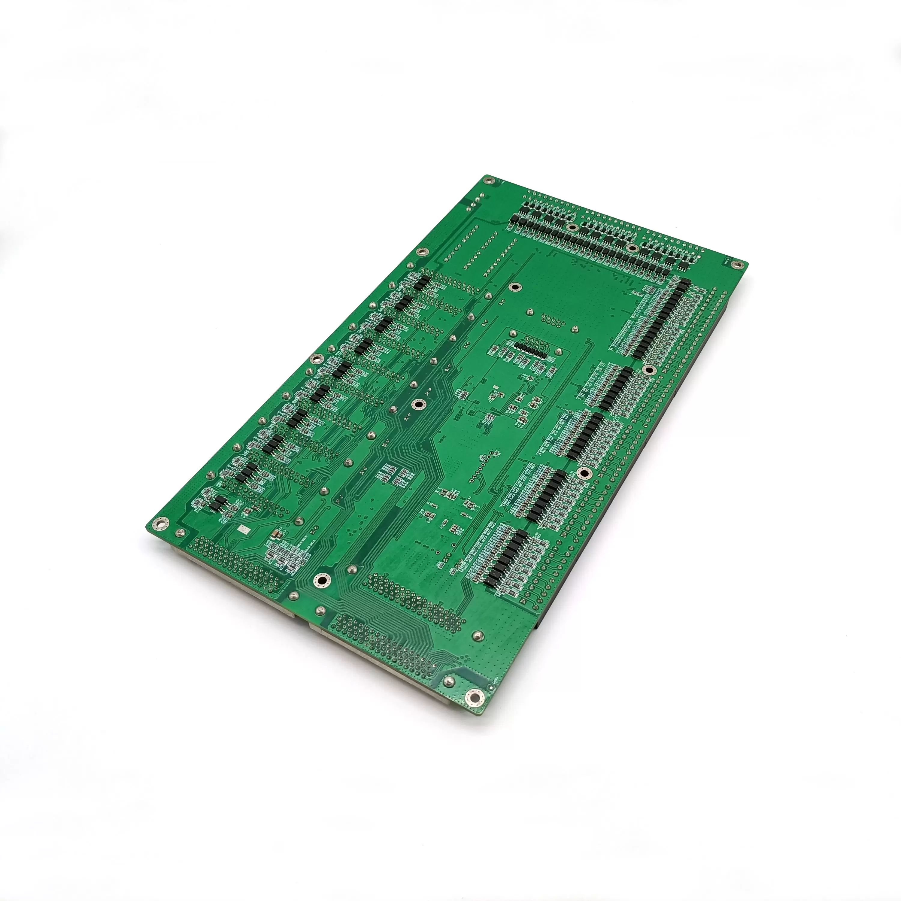
HDI PCB Design lets you make smaller electronic products. These products can be faster and more reliable. You can fit more circuits in a small space. This helps your devices work better and last longer. Many companies pick this technology for higher pin counts. It also helps keep products working well. If you care about quality and reliability, you build a strong base for every project. Benlida does this for their work. Try to solve problems when you design and use technology.
Key Takeaways
HDI PCB Design helps make electronics smaller and faster. It also makes them more reliable by fitting more circuits in less space.
Picking the right layer stack-up is very important for good signals and power. Plan your stack-up early so you do not have problems later.
Use good routing strategies to keep signals clean and lower interference. This helps the board work better.
Choose strong materials that fit your design needs. This affects how strong, reliable, and good at handling signals the board is.
Testing and working with manufacturers is very important. Talking early helps find problems and makes production easier.
HDI PCB Design Overview
What Is HDI PCB Design?
You use HDI PCB Design to fit more circuits in less space. HDI means High-Density Interconnect. This design uses things like microvias and thin lines. These help make boards small and light. You can look at the table to see how HDI and regular PCBs are different:
Comparison Factor
HDI PCBs
Traditional PCBs
Layer Count
More layers, up to 16+
Fewer layers, ≤6
Via Design
Blind, buried, microvias
Mostly through-hole
Signal Integrity
Better
Lower
Functionality
Higher
Lower
Complexity and Cost
Higher
Lower
HDI PCB Design uses special materials and careful drilling. This gives you better signal paths and stronger boards. These boards work well in fast and reliable devices.
Why HDI Matters in Electronics
You find HDI PCB Design in many new electronics. Phones, computers, and cars use this technology. In the last ten years, more people want HDI boards. Companies want products that are smaller, faster, and work better. HDI boards help them do this.
Signal integrity gets better because HDI makes signal paths shorter.
Impedance control is easier with laser-drilled microvias.
Boards stay strong even when it is hot.
Tip: Using HDI PCB Design helps your products last longer and work better.
Many industries pick HDI for high-performance needs. For example, AI servers and cars need these special boards. HDI technology is changing how electronics are made.
Design Considerations
Layer Stack-Up Optimization
When you start HDI PCB Design, you pick the right layer stack-up. This choice decides how your board handles signals and power. There are many common stack-up types in high-speed designs. The table below shows some popular ways to arrange layers:
Stack-Up Type
Layer 1
Layer 2
Layer 3
Layer 4
Layer 5
Layer 6
Layer 7
Layer 8
4-Layer Stackup 1
Signal (Top)
Ground (GND)
Power (VCC)
Signal (Bottom)
N/A
N/A
N/A
N/A
4-Layer Stackup 2
Signal
Ground
Ground/Power
Signal
N/A
N/A
N/A
N/A
6-Layer Stackup 1
Signal
Ground
Signal
Signal
Power
Signal
N/A
N/A
6-Layer Stackup 2
Signal
Ground
Power
Ground
Signal
Signal
N/A
N/A
8-Layer Stackup 1
Signal
Ground
Signal
Power
Ground
Signal
Ground
Signal
8-Layer Stackup 2
Signal
Ground
Signal
Power
Power
Signal
Ground
Signal
If you put ground and power planes close to signal layers, you get better signal integrity. This setup helps lower noise and crosstalk. It also helps control heat and keeps impedance right for fast signals. Benlida uses advanced tools to build these stack-ups very carefully. This means your boards work well and last a long time.
Tip: Plan your stack-up early. This helps you avoid signal problems and makes building the board easier.
Routing Strategy
You need a good routing strategy for HDI PCB Design. Good routing keeps signals clean and stops interference. The table below lists top routing strategies and their benefits:
Strategy
Explanation
Utilize guard traces
Guard traces shield signals and lower crosstalk.
Increase spacing between traces
Wider spacing reduces coupling and interference.
Implement solid ground planes
Solid ground planes give signals a clear return path and cut down EMI.
Use differential signaling
Differential pairs boost noise immunity and lower crosstalk.
Incorporate shielding techniques
Shields and cages block electromagnetic radiation.
Use via stitching
Via stitching connects ground planes and improves signal return.
These strategies help you fit more circuits in a small space. HDI PCB Design lets you route complex signals in tiny areas. You see this in phones and tablets. Benlida’s engineers use these methods to make boards that pass tough quality checks.
Note: Advanced routing lets you add more features to small boards without losing performance.
Component Placement
You need to place components carefully in HDI PCB Design. Smart placement makes your board easier to build and keeps it strong. Here are some best practices for placing components:
Best Practice
Description
Strategic Component Placement
Place parts to lower signal interference and boost routing density.
Use of Blind and Buried Vias
These vias connect layers without taking up much space.
Prototyping and Testing
Test your layout before mass production to catch problems early.
You also use microvias to move signals between layers. You should not use microvias across too many layers to keep your board strong. Spread out hot parts and put them near thermal vias or heat sinks to manage heat. Leave enough space between parts so heat does not build up.
Tip: Always test your layout with prototypes. This helps you find and fix problems before you make many boards.
Material Selection
You pick materials that fit your design needs. The right material keeps your board strong and helps it work well. The table below shows important things to check when picking materials:
Criteria
Description
Decomposition Temperature (Td)
Pick materials with high Td to avoid breakdown during use.
Coefficient of Thermal Expansion
Match CTE with other parts to stop cracks and warping.
Thermal Conductivity (k)
High thermal conductivity helps move heat away fast.
Suitability for Laser Drilling
Materials must handle laser drilling and keep their shape.
RoHS Compliance
Use eco-friendly, lead-free, and halogen-free materials.
Key Material Properties
Check for signal loss, operating frequency, and strength.
High-performance materials cost more but make your board last longer. Standard materials are cheaper but may not work as well in tough jobs. Benlida uses top-quality materials and checks every batch to meet strict rules.
Note: The material you pick changes the cost, reliability, and how well your board handles signals and heat.
Signal Integrity
You protect signal integrity in HDI PCB Design by planning your layout and stack-up. You face problems like crosstalk, impedance mismatches, and signal delay. Keep traces apart and use solid ground planes to lower interference. Use simulation tools to check signal paths and timing. These tools help you find problems before you build the board.
You want impedance to stay the same, usually between 50 and 100 ohms, for fast signals. Watch for power integrity problems, especially with split ground and power planes. Benlida’s quality team uses advanced tests to make sure every board meets signal rules.
Tip: Use simulation software to check your design for signal problems. This step saves time and money.
Careful design and strong manufacturing make HDI PCB Design reliable. You get boards that work well in tough jobs.
HDI PCB Design Technologies
Microvias and Interconnects
Microvias connect layers inside HDI PCBs. Some microvias are only 50 micrometers wide. Lasers drill these tiny holes. CO2 and UV lasers make smooth microvias. Filled microvias help send more signals. They also make electrical performance better.
Microvias can be just 2 mils wide. Capture pads are 6-8 mils.
Thin dielectric layers and thin copper foil keep sizes exact.
Stacked microvias like NextGen-SMV® allow tricky designs. They also help finish boards fast.
Microvias make signal paths shorter. This keeps signal integrity strong. It also lowers signal loss. Small microvias cut down parasitic capacitance and inductance. This helps your board work faster.
Fine-Line Traces
Fine-line traces fit more circuits in less space. Trace widths and spacing can be as small as 0.075 mm (3 mil). This makes boards small and powerful.
Feature
Minimum Width/Spacing
Fine Line & Spacing
0.075 mm (3 mil)
Use 0.003" trace width and spacing for 1 oz. copper.
Use 0.005" for 2 oz. copper.
Use 0.009" for 3 oz. copper.
Use 0.010" for 4 oz. copper.
Fine-line traces let you route signals close together. This boosts performance and helps miniaturization. You can add more parts and keep signals fast. Differential pairs in fine-line routing keep signal quality high.
Advanced Materials
Advanced materials are needed for HDI PCB Design. High-frequency substrates keep signal integrity strong. Low-loss laminates help control heat. Flexible materials make boards light and small. Polyimide films and ceramic-filled materials make boards tough.
High-performance materials lower mechanical stress when things get hot.
These materials work well for high-frequency jobs like 5G and IoT.
Buildup layers from advanced materials keep signals strong in fast computers.
Thermal conductivity moves heat away from hot spots.
High thermal conductivity materials stop overheating.
Standard FR-4 may not work for high-power jobs.
Material Type
Thermal Conductivity
Application
Enhanced Laminates
High
Power electronics, LED applications
Standard FR-4
0.3 W/m·K
General use
Advanced materials help with heat, signal integrity, and strength.
Design Software Tools
Good software helps you design HDI PCBs. Some popular tools are:
Altium Designer is good for advanced boards.
Allegro PCB Designer has strong layout features.
Ansys RedHawk checks power and signal integrity.
Autodesk EAGLE is easy to use.
DipTrace helps with schematic capture.
Feature
Description
Vias
Blind and buried vias save space and help signals.
Component Selection
Pick SMD and BGA parts to set trace widths and via types.
Material Selection
Choose materials for easy building and good performance.
Design Reviews
Get feedback early to find mistakes.
You can use these tools to plan layouts, test signals, and check for mistakes. This helps you make boards that work well.
Best Practices
HDI PCB Design Best Practices
You can get good results in HDI PCB Design by using smart steps. These steps help you stop mistakes and make your product work better and last longer.
Optimize Your Layout Design Put parts in the right spots and plan paths well. This makes building easier and helps your board last.
Use Advanced Software Tools Pick tools that let you see and test hard connections. These tools help you find problems before you make the board.
Work Together with Your Team Show your design to your team early. Working with engineers and builders helps you find problems fast.
Pick the Right Materials Choose materials that fit your project. Good materials help your board last and waste less.
Follow DFM Guidelines Plan for easy building from the start. This keeps your board simple to make and high in quality.
If you use these steps, your products will last longer and work better. You also lower the chance of problems when making your boards.
DFM Guidelines
Design for Manufacturability (DFM) means you plan your board so it is easy to build. Good DFM steps help you stop mistakes and save money. Here are some important rules:
Guideline
Description
Annular Ring Size
Use at least 0.05 mm (2 mil) for outside layers. You can allow up to 20% less for small flaws.
Blind Vias Aspect Ratio
Keep the ratio at 0.75:1. This helps copper stay even and strong.
Material Selection
Pick materials with Tg of 200°C or more. These can handle heat and laser drilling.
Positive Etchback
Use positive etchback for strong links, as IPC-6012 class 3 needs.
Place and turn parts for easy building.
Plan for good heat control to keep your board safe.
Leave space between parts to stop short circuits.
If you follow these DFM rules, you will have fewer mistakes and smoother building.
Collaboration with Manufacturers
You get better boards when you work with your builder. Early talks with your builder help you make sure your design can be built. Here is how you can make your project better:
Meet with your builder early to check if your design works.
Review your design often with your team. This helps you find and fix problems before they get big.
Keep clear and open talks. Share updates and ideas with everyone.
Benlida believes in teamwork and open talks. This way, you avoid delays and costly changes.
Quality Control and Testing
Testing and checks are important for strong and reliable boards. You should use many tests to make sure your HDI PCB works well in real life.
Testing Method
Description
Temperature Cycling Tests
Check if your board can handle big temperature changes. This test shows if microvias stay strong.
Thermal Stress (Shock) Testing
Test your board with fast heat changes. This finds weak spots that could break during soldering or use.
High Temperature/Humidity Bias Testing
Put your board in hot, wet places. This checks if insulation and microvias stay strong under stress.
Benlida uses advanced tests and strict checks at every step. This makes sure you get boards that meet high standards.
When you use these smart steps, you make boards that last longer and work better. You also show you care about quality and making customers happy.
Challenges and Solutions
Manufacturing Constraints
When you make HDI PCBs, you face many challenges. These boards need careful planning and high accuracy. Here are some common problems you might see:
Design is harder because layouts are more complex.
You need special machines for high accuracy.
Making these boards can take more time.
If you skip steps, you might get more defects.
You cannot use many through-hole parts, so you use more surface-mount ones.
You must check quality closely to find small mistakes.
Microvias make things trickier and need special drilling.
You have to keep signal integrity high for fast circuits.
You can fix these problems by talking with your manufacturer often. Use advanced tools to help you. Review your work early and talk clearly to avoid mistakes.
Reliability Issues
HDI PCBs are strong if you use good materials and methods. These boards can handle heat, shaking, and tough places. For example, HDI PCBs in planes can work from -40°C to 85°C. Good HDI PCBs can have very low failure rates, like 0.1%. Many layers spread out stress, so cracks and delamination happen less after heating and cooling.
Tip: Test your boards in real life to make sure they last.
Cost Management
You can save money on HDI PCB projects by being smart:
Make your design use space and materials well.
Buy parts in a smart way to stop delays and extra costs.
Pick the best way to make your boards.
Talk with suppliers to get better prices.
Use good design steps and automation tools.
Outsource design if it saves time and money.
Make more prototypes at once to save on setup.
Ask for tooling credits if you order a lot.
Use test jigs to check boards faster.
These steps help you keep costs low and make good products.
Troubleshooting
You might have problems when making HDI PCBs. Here are ways to fix them:
Use automated optical inspection to find open or short circuits.
Use X-ray inspection to look for hidden solder problems.
Check your design files for mistakes before making boards.
Test boards in different temperatures and humidity.
Work with your manufacturer to fix problems fast.
Note: Fixing problems quickly keeps your project on time and makes boards reliable.
Case Studies
Consumer Electronics Success
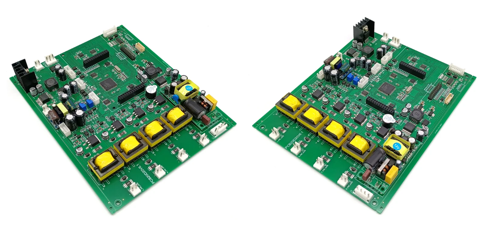
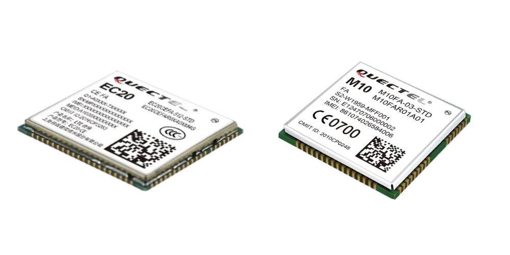
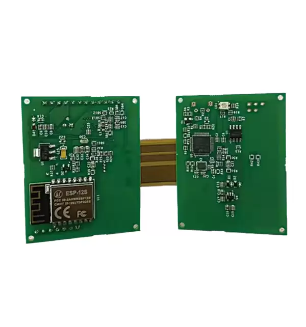
You can find HDI PCB technology in many things you use. Phones, tablets, and smartwatches all have HDI PCBs inside. These boards help make your devices small and light. They also help your devices work faster. For example, a phone needs to fit a camera, battery, and processor in a thin case. HDI PCBs let more circuits fit in less space, so this is possible.
Benlida works with electronics brands to make good HDI PCBs. You can count on their boards to handle fast signals and high power. Their advanced factories keep your devices working well, even if you use them a lot.
Key Benefits in Consumer Electronics:
Your battery lasts longer because power is used well.
You get faster data for smooth video and games.
Devices are thinner and easy to carry.
There are fewer problems because of strong checks.
Tip: If you pick HDI PCBs for your products, people get better devices that last longer.
Industrial Applications
You also see HDI PCBs in factories, medical tools, and cars. These boards help machines work well in hard places. For example, a robot arm in a factory must move fast and stay cool. HDI PCBs help by moving heat away and keeping signals clear.
Benlida helps factories by making strong and reliable boards. Their HDI PCBs pass tough tests for heat, shaking, and wetness. You can use these boards in control systems, sensors, and power supplies.
Common Uses in Industry:
Application
Why Use HDI PCBs?
Factory Automation
Handles fast signals and heat
Medical Devices
Fits in small, complex equipment
Automotive Systems
Survives vibration and temperature
Note: HDI PCBs help your machines last longer and stay safe, even in tough places.
You can do well in HDI PCB Design if you care about quality and reliability. Use advanced manufacturing to help your boards work better. First, make a clear plan before you start. Pick the best materials for your board. Test your boards to make sure they work right. Here is a checklist you can use:
Plan your layout early
Pick high-quality materials
Work with your manufacturer closely
Test your board for reliability
You can look at Benlida’s one-stop PCB & PCBA services as a good example for quality and working fast.
FAQ
What is the main benefit of HDI PCB design?
You can fit more circuits in a smaller space. This makes your devices lighter and faster. HDI PCBs help your products work better and last longer.
How do microvias improve HDI PCBs?
Microvias make signal paths shorter.
Benefit
Result
Shorter paths
Faster signals
Less interference
Stronger signals
Why should you choose high-quality materials for HDI PCBs?
You get stronger boards that last longer. High-quality materials help your board handle heat and keep signals clear.
How does Benlida ensure quality in HDI PCB manufacturing?
Benlida uses advanced machines and strict tests. You get boards that meet high standards for reliability and performance.
Can HDI PCBs be used in cars and medical devices?
Yes. You see HDI PCBs in cars, medical tools, and factory machines. These boards work well in tough places and help keep devices safe.
This website uses cookies to provide you with a safer and more personal experience. By accepting, you agree to the Cookie Policy and the use of cookies for advertising and analytics purposes.
 en
en


 WhatsApp