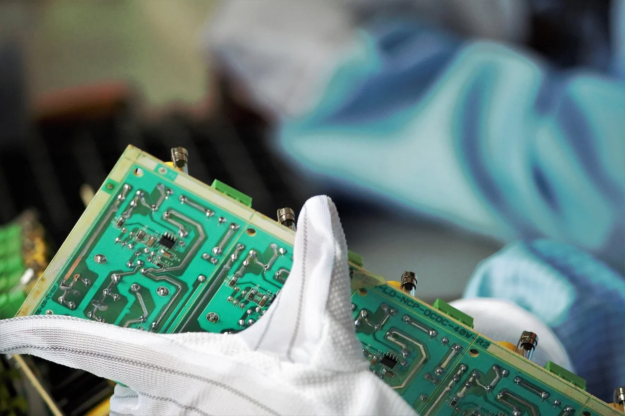
The dimension of modern electronics getting smaller and integrates more complex circuits. The progress often comes down to one “quiet” PCB manufacturing process that determines the integration: PCB lamination. If lamination is done well, the layers could perform like a stable structure. If it’s not properly done, there might be hidden defects—voids, de-lamination, warpage, misalignment—that don’t always show up until the electronic product fails.
If you’re looking for a PCB Fabrication Service, it’s better to understand lamination beyond the textbook definition. This guide explains the PCB lamination process in plain language, then goes deep into materials, parameters, defects, quality control, and design tips—support you to make better engineering and purchasing decisions.
1. PCB Lamination Explained in 60 Seconds
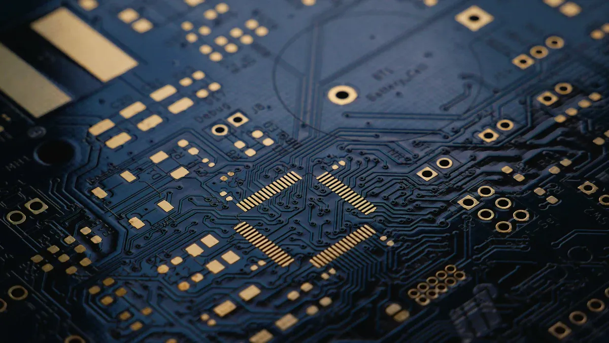
PCB lamination is the process of bonding multiple circuit layers into a single solid board using heat, pressure, and resin (usually in prepreg). Lamination exists mainly in multilayer PCBs, because multiple etched inner layers must be permanently fused together to create one mechanically stable, electrically reliable structure.
A simple analogy: think of lamination like making a high-performance “layer cake,” except the glue is engineered resin, the layers are copper circuits, and the oven is a precision press cycle. Going through correctly and properly, the resin flows and cures uniformly, locking layers in place without voids or misalignment.
Lamination vs sequential lamination:
Standard lamination bonds the full stack in one main press cycle.
Sequential lamination bonds the board in stages (common in HDI) to enable microvias and complex interconnect structures.
2. Why PCB Lamination Is the Backbone of Multilayer PCB Manufacturing
In multilayer PCBs, lamination is the moment the board becomes a unified structure. Once laminated, inner layers are “locked in” and everything downstream—drilling, plating, outer-layer imaging—depends on that structure.
What happens if lamination fails?
Lamination defects often create hidden reliability risks:
resin voids could reduce dielectric integrity and weaken thermal/mechanical stability
delamination could spread under thermal cycling
warpage could cause assembly problems and premature solder joint fatigue
misalignment could reduce annular rings and weaken vias
How lamination affects performance
Electrical reliability: stable dielectric thickness and controlled resin distribution support predictable impedance and insulation performance.
Mechanical strength: good bonding prevents cracking and layer separation under vibration or bending stress.
Long-term field performance: laminated boards will encounter repeated thermal cycles, humidity exposure, mechanical shocks, and constant power-on heat.
Yield, cost, and why buyers should care
A lamination issue usually far beyond rework or repair. It often becomes a scrap and fatal problem. That’s why lamination quality directly leads to:
yield (first-pass success rate)
schedule stability
total project cost (especially for complex multilayer and HDI builds)
3. PCB Lamination vs Other PCB Manufacturing Processes
Understanding what lamination by compare with other manufacturing process.
Lamination vs etching
Etching creates copper patterns on individual layers. Lamination is what turns those independent layers into a single board. Without lamination, multilayer conductivity and mechanical stability are impossible.
Lamination vs drilling
Drilling creates holes for vias and leads, but drilling happens after standard multilayer lamination because the board must be structurally stack up first. (Sequential lamination changes this timing in HDI builds.)
Lamination vs PCB assembly (PCBA)
Lamination is a process of FAB (fabrication). PCBA is the later process which mounts components on PCB. Many “assembly failures” actually start earlier: a warped laminated PCB could cause alignment issues, tombstoning, or solder joint stress.
Where lamination fits
A simplified timeline looks like:
Design files → inner-layer imaging/etching → lamination → drilling → plating → outer-layer imaging → solder mask → surface finish → profiling → test → shipment
4. PCB Types That Require Lamination (With Real Use Cases)
4.1 Multilayer rigid PCBs (4–20+ layers)
This is the classic lamination application case. Multilayer PCBs are common in:
consumer devices with dense routing and compact footprints
industrial controllers that need stable performance and longer life cycles
communication hardware where signal integrity matters
4.2 Double-sided PCBs (why lamination may still be needed)
In some double-sided stackups, a lamination-like bonding stage can still exist (depending on build style, materials, and insulation structure). The key difference: the complexity and risk profile are lower than true multilayer stacks, but resin flow and thickness control still matter.
4.3 Sequential lamination boards (HDI PCBs)
HDI often uses sequential lamination to enable:
blind/buried vias
microvias
via-in-pad structures for fine-pitch BGAs
These designs demand tight registration and strong control over resin flow and curing across multiple cycles.
4.4 High-frequency & RF PCBs (PTFE / Rogers)
RF laminates often perform differently than standard FR-4. At microwave frequencies, small variations in dielectric thickness or bonding quality can change performance. Lamination control becomes critical for:
stable dielectric properties
reduced void risk
consistent impedance and insertion loss behavior
5. PCB Lamination Materials Breakdown (Designer-Focused)
Designers often take lamination as “the factory’s job.” In reality, material choices determine whether lamination is easy, difficult, or risky.
5.1 Core materials
FR-4: general-purpose, widely applied for many PCBs.
High-Tg epoxy: better thermal stability for higher temperatures and tougher assembly cycles.
Polyimide: often applied where flexibility or higher temperature performance is needed.
PTFE / RF laminates: low loss and stable dielectric behavior, but lamination requires careful control due to material characteristics.
5.2 Prepreg materials
Prepreg is fiberglass + partially cured resin. In lamination, prepreg becomes the “bonding medium.”
Key factors:
resin system type
flow characteristics (how it fills gaps and bonds copper surfaces)
thickness control (affects dielectric thickness and impedance)
5.3 Copper foil
Copper choices influence pressure and deformation risk.
Standard copper is common and cost-effective.
Rolled copper can be beneficial in certain structures (including dynamic or flex-related designs).
Copper weight impacts:
required pressure balance
resin flow behavior around copper features
risk of print-through or uneven thickness
5.4 Auxiliary materials
These don’t become part of the final board, but they influence lamination results:
Caul plates: distribute pressure and heat evenly
Release films: prevent sticking and contamination
Metal sustaining foils: help stabilize pressure distribution in specific builds
Competitors often skip these details, but they’re part of why two factories can build the same stack-up and get different yields.
6. PCB Lamination Process Step-by-Step (Concise & Visual)
Here’s a clear view of the standard PCB lamination process for multilayer boards:
Inner layer preparation and surface treatment
Inner layers are etched and inspected, then treated to improve bonding (surface conditioning).
Stack-up layup and alignment
Cores and prepregs are stacked in the correct order, aligned to tooling holes or registration systems.
Vacuum sealing and air removal
Vacuum helps remove trapped air, reducing void risk and improving resin fill.
Heat and pressure lamination cycle
Heat softens resin; pressure forces resin to flow, fill gaps, and bond layers. Then the resin cures into a solid matrix.
Controlled cooling
Cooling is not a passive step. Cooling rate affects internal stress and warpage.
Post-lamination degassing and inspection
Boards may go through stabilization steps and are checked for thickness, warpage, and bonding quality.
7. Key PCB Lamination Parameters and Their Effects
7.1 Lamination temperature
Temperature must match the resin system. Too low might cause under-curing, weak bonding, and later delamination. Too high might cause resin degradation, excessive flow, or stress.
7.2 Lamination pressure
Pressure determines resin flow and contact quality. Not-enough pressure will leave voids, but too much pressure leads to:
● squeeze resin out unevenly
● deform copper features
● increase risk of thickness non-uniformity
7.3 Lamination time
Time determines cure completeness. Shortening cycles aggressively may increase throughput but also increase defect risk if the resin doesn’t fully cure.
7.4 Cooling rate
Cooling affects:
● warpage and bow
● internal stress in the resin system
● stability of dielectric thickness
Controlled cooling is one of the most practical ways to prevent “mystery warp” that shows up during assembly.
Lamination is one of the few PCB fabrication steps that can’t be “rushed” without consequences. Even if imaging and drilling are ready to go, a multilayer PCB can’t move forward until the press cycle is complete, the resin is fully cured, and the panel has cooled in a controlled way. That’s why lamination often becomes the schedule gate in multilayer production.
Typical lamination cycle times (what’s included)
When people ask “how long does lamination take,” they often picture only the hot-press stage. In reality, lamination time usually includes:
● Layup and alignment (stack building and registration)
● Vacuum / de-airing (removing trapped air to reduce voids)
● Heat-up + cure dwell (resin flow and full polymer cure)
● Controlled cooling (to prevent warpage and internal stress)
● Post-lamination stabilization + basic inspection (thickness/warp checks before the next process)
So the "lamination cycle" is a full sequence, not one timer setting.
Layer count vs cycle duration (why thicker isn’t just “a little slower”)
As layer count increases, lamination tends to take longer for three reasons:
More thermal mass: thicker stacks heat and cool down slowly, and uniform temperature through the panel matters for cure consistency.
More resin behavior to manage: more interfaces means more potential for uneven resin flow or trapped air if the profile isn’t optimized.
Tighter yield protection: high-layer PCBs are costlier to scrap, so manufacturers typically use more conservative, stability-focused cycles.
Result: higher layer count often means longer press time + longer cooling + more verification, not just “a slightly longer cure.”
Sequential lamination time penalties (HDI reality)
For HDI and complex via structures, sequential lamination can add significant lead time because it’s essentially lamination in multiple rounds:
● build and laminate the base stack
● drill/plate microvias or create interconnect features
● laminate additional layers
● repeat as required
Each round brings its own cycle time plus handling, registration control, and inspection. The time penalty isn’t only the extra press cycles—it’s also the extra opportunities for warpage control and alignment verification between stages.
How lamination delays cascade into downstream steps
If lamination runs late or needs a re-run, it pushes back almost everything that follows:
Drilling: drilling schedules depend on laminated panels being stable and flat. Warpage control and thickness confirmation often determine when drilling can start.
Plating: through-hole metallization and copper plating can’t proceed until drilled holes exist—so plating is directly queued behind lamination + drilling.
Solder mask: solder mask is near the end of the fabrication flow. Any upstream slip (lamination → drilling → plating → imaging) compresses the window for solder mask curing and final inspection.
9. Common PCB Lamination Defects and Root Causes
Delamination: weak bonding caused by under-cure, contamination, incompatible materials, or poor process control.
Resin voids: trapped air or insufficient resin fill; often linked to vacuum control and layup conditions.
Poor layer adhesion: surface treatment issues, contamination, or incorrect cure profile.
Warpage and bow: asymmetric stack-ups, uneven copper distribution, or cooling stress.
Inner-layer misalignment: registration errors during layup, material movement, or cumulative distortion.
10. PCB Lamination Quality Control and Inspection Methods
Lamination defects are often internal—you can’t “see” them from the surface. That’s why good manufacturers treat lamination quality like a verification problem: measure the structure, confirm adhesion, and stress the PCB in controlled methods, to expose weak bonding before it go for assembly.
Microsection analysis (cross-section verification)
Microsectioning is one of the most direct ways to evaluate lamination quality. A small coupon is cut, mounted, polished, and inspected under a microscope to confirm:
● layer-to-layer bonding and resin fill
● voids, delamination indicators, or resin starvation
● dielectric thickness consistency (important for impedance and insulation margins)
● alignment quality between inner layers (registration)
This is often the “proof” step when buyers ask how lamination quality is validated.
Peel strength testing (bond integrity check)
Peel tests evaluate how strongly copper and dielectric layers adhere after lamination. It helps to confirm:
● proper curing (not under-cured, not brittle from over-stress)
● adequate surface treatment/oxide replacement performance
● stable bonding across batches and material lots
Strong peel performance generally correlates with better resistance to delamination during thermal cycling and reflow.
Warpage measurement (flatness and stress control)
Warpage and bow are practical production risks—especially for assembly. Measurement typically checks:
● panel flatness after lamination and after subsequent thermal exposure
● whether warpage stays within acceptable limits for component placement and soldering
● trends by layer count, copper balance, or material selection
This is a key gate because even “electrically fine” boards can become unbuildable if flatness is unstable.
X-ray inspection (internal anomaly screening)
X-ray is useful for identifying certain internal issues without destructive cutting, such as:
● void patterns in resin-rich regions
● layer shift indicators in specific structures
● anomalies that may later affect drilled hole registration or via reliability
It’s especially valuable when combined with microsection data—X-ray can screen, microsection can confirm.
Thermal stress testing (reliability under heat cycling)
Lamination must survive real operating conditions and assembly heat. Thermal stress testing helps expose:
● weak bonds that open up under temperature swings
● early delamination
● stability problems that only appear after heat exposure (reflow simulation or cycling)
For high-reliability PCBs, this type of testing is often what separates “passes today” from “survives for years.”
11. Advanced PCB Lamination Technologies (Modern Techniques)
11.1 Sequential lamination for HDI PCBs
To build complex via structures stage-by-stage.
11.2 ALIVH (Any Layer Interstitial Via Hole)
Any-layer concepts push density further but demand extremely stable lamination and via formation control.
11.3 Vacuum-only lamination
Vacuum-focused approaches reduce void risks and improve resin fill consistency in challenging process.
11.4 Rapid-cure and nano-resin systems
New resin chemistries aim to reduce cycle times and improve thermal/mechanical performance—useful, but must be validated carefully.
11.5 Embedded components during lamination
Embedding components can reduce size and improve performance in certain designs, but it raises lamination complexity and inspection requirements significantly.
12. Design Tips to Improve PCB Lamination Success
Most lamination issues don’t start in the press—they start in the stack-up decisions and the way requirements are communicated. If you design with lamination and verify through design regulations, you’ll get better yield, flatter panels, and fewer “unexpected” defects.
Stack-up symmetry rules (warpage prevention first)
Symmetry is the simplest way to reduce internal stress:
● Build the stack so the top half balance the bottom half (layer count, dielectric thickness, copper weight).
● Keep core/prepreg distribution balanced around the center.
● If must run asymmetric constraints (connectors, shields, special layers), flag it early—manufacturers may need compensation strategies.
Material compatibility checks (don’t mix casually)
Lamination success depends on how materials behave together under heat and pressure:
● Confirm that resin systems and Tg targets are compatible across the stack.
● For mixed material builds (e.g., RF + FR-4 hybrids), align on bonding sheets / prepreg selection and the press profile that supports both.
● Call out any special requirements (low-loss laminates, high-temperature operation, harsh environments) so the material set is chosen intentionally, not by default.
Copper balance strategies (control resin flow + thickness uniformity)
Copper density isn’t only an electrical decision—it affects lamination stability:
● Avoid extreme copper imbalance between layers; it can drive uneven resin flow and thickness variation.
● Use copper thieving / balancing patterns when needed to reduce large open-resin areas.
● For heavy copper or localized thick copper regions, plan for higher lamination complexity and discuss pressure/resin flow considerations with the factory.
When to avoid excessive layer counts (complexity tax is real)
More layers can solve routing problems, but they also add:
● Longer lamination cycles and higher cumulative stress
● Tighter registration difficulty
● Greater scrap cost if a defect occurs
If the design doesn’t truly need the extra layers, consider alternatives like HDI fanout, better component placement, or routing strategy changes—you can hit the same performance target with lower build risk.
Communicating lamination requirements to manufacturers (make it “buildable”)
The fastest route to stable lamination is clear documentation. Provide:
● A complete stack-up drawing (materials, thickness targets, copper weights)
● Controlled impedance requirements and where they apply
● Special notes for hybrids, HDI structures, via-in-pad, or tight warp limits
● Acceptance criteria: warpage limits, thickness tolerance, any reliability test expectations
When the manufacturer understands what’s critical (and why), they can choose the right press profile, materials, and inspection plan—before production starts.
13. How to Reduce PCB Lamination Time Without Sacrificing Quality
Reducing time is about smarter planning, not simply shortening cure:
Material selection strategies: choose resin systems that support stable cycles for your use case
Press cycle optimization: refine temperature ramps and pressure profiles within validated windows
Batch planning: group builds with similar materials and thickness to reduce changeover instability
DFM collaboration: manufacturer input often prevents redesign loops that cost more time than any press cycle ever will
14. PCB Lamination FAQs
1. What temperature is used for PCB lamination?
It depends on the resin system and material set. The correct range is defined by material specifications and validated process windows.
2. How long does PCB lamination take?
The press cycle plus controlled cooling can be significant. More layers and special materials typically increase cycle time.
3. Why do multilayer PCBs warp?
Common causes include stack-up asymmetry, copper imbalance, and stress from cooling rate or material mismatch.
4. Can lamination defects be repaired?
Some defects are non-repairable once laminated, that’s why prevention and inspection are critical.
5. Is lamination required for all PCBs?
Lamination is primarily associated with multilayer structures; single-layer boards don’t require it in the same way.
15. Conclusion: Why PCB Lamination Determines PCB Reliability
PCB lamination is where a multilayer PCB board becomes a single, stable structure—so it directly sets the ceiling for reliability. Technically, lamination quality influences inner-layer alignment, dielectric consistency, via durability, and warpage control. From a business perspective, it affects yield, rework risk, and delivery schedule—especially on high-layers and HDI builds where one hidden defect can ruin the entire panel even the whole batch.
That's why manufacturer expertise matters. A capable supplier doesn’t treat lamination as a “standard press step”—they manage materials, profiles, vacuum control, cooling, and inspection as a system, with clear process windows and repeatable quality verification.
If you're looking for a partner for multilayer PCB fabrication, the fastest way to reduce project risk is to work with a team that can align stack-up intent with real production control. For Benlida's PCB fabrication capabilities and board categories, you can explore the PCB Fabrication Service here.
Related PCB manufacturing processes
PCB Manufacturing Process Step-by-Step
PCB Inner Layer Imaging & Etching Process
How do drilling (mechanical/laser) processes work in PCB manufacturing?
What is the plating process in PCB Manufacturing?
How are vias formed in PCBs?
How is solder mask applied on PCB?
Ultimate Guide to PCB silk screen printing process
What is the surface finish process in PCB?
What are the most common methods of PCB testing?
About the auther:

Sonic Yang
As a major of Electronics and Mechanical Automation, Sonic has been engaged in PCB design, R&D, manufacturing of eletronics for around 22 years, as engineering director and coordinates with supply chain(components&CNC parts), providing professional supports and consults for global customers.
 en
en

 WhatsApp