Introduction: The Rise of Ceramic PCB Manufacturing
In an era where electronics are getting smaller, faster, and more thermally demanding, ceramic PCBs have become the gold standard for performance and reliability. Compared to traditional FR-4 substrates, ceramic printed circuit boards offer dramatically higher thermal conductivity (up to 220 W/m·K) and exceptional stability across extreme temperatures — from –55 °C to 800 °C and beyond.
These properties make them indispensable for mission-critical applications in aerospace, automotive power modules, 5G base stations, and industrial automation systems. But what truly sets ceramic PCBs apart lies not just in their material composition — it’s the precision manufacturing process behind them.
In this article, we’ll break down the key processes involved in ceramic PCB manufacturing, the materials used, and why precision engineering is crucial for consistent high performance.
For detailed product options and technical data, you can visit Benlida's Ceramic PCB page.
Understanding the Structure of Ceramic PCBs
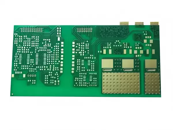
A ceramic PCB is typically made from a single-layer or multilayer ceramic substrate such as Alumina (Al₂O₃), Aluminum Nitride (AlN), or Silicon Carbide (SiC). Unlike organic boards like FR-4, which rely on glass fiber and epoxy resin, ceramic PCBs are inorganic, offering excellent heat dissipation, electrical insulation, and dimensional stability.
The typical structure consists of:
Ceramic Base Layer: Provides mechanical strength and thermal management.
Metal Layer (Copper, Silver, or Gold): Conducts current and forms the circuitry.
Protective Coatings: Applied for oxidation resistance and solderability.
These materials are processed through specialized techniques such as Direct Bonded Copper (DBC), Direct Plated Copper (DPC), or Thick-Film Printing, each serving unique performance requirements.
1. Direct Bonded Copper (DBC) Process
The DBC process is one of the most popular methods for creating power electronic ceramic PCBs. It involves bonding a thick copper sheet (typically 100–400 µm) directly onto a ceramic substrate at high temperature.
Steps Involved:
Oxidizing Copper Foil: A thin oxide layer forms on the copper surface.
High-Temperature Bonding: The copper and ceramic are heated (around 1,060 °C), allowing oxygen atoms to diffuse and create a strong chemical bond.
Circuit Etching: The copper layer is then patterned using photoresist and etching to form circuit traces.
Advantages:
Excellent thermal conduction between copper and ceramic.
Strong mechanical adhesion without adhesives.
Ideal for high-current, high-temperature devices such as inverters and motor drives.
Applications: Power modules, IGBT circuits, and automotive power controllers.
2. Direct Plated Copper (DPC) Process
DPC technology uses sputtering and electroplating to deposit thin copper layers onto ceramic substrates, achieving high circuit density and fine line features.
Process Steps:
Surface Preparation: Cleaning and activating the ceramic surface.
Seed Layer Deposition: A very thin layer of metal (often tungsten or molybdenum) is sputtered onto the ceramic.
Electroplating Copper: Copper is electroplated to the desired thickness (10–50 µm).
Photoresist Patterning and Etching: Circuit traces are defined for micro-scale accuracy.
Benefits:
Supports fine-line circuitry (<50 µm line width).
Enables multilayer and high-density interconnect (HDI) structures.
Lower processing temperature than DBC, minimizing thermal stress.
Applications: RF modules, 5G communication systems, LED arrays, and sensors.
3. Thick-Film Printing Process
The thick-film process is an established technique for creating conductive, resistive, and dielectric layers on ceramic boards through screen printing.
How It Works:
Printing: Conductive pastes (containing silver, gold, or copper particles) are screen-printed onto the ceramic surface.
Drying and Firing: The printed layer is fired at high temperatures (850–900 °C) to fuse the metal with the ceramic.
Multilayer Stacking: Multiple conductive and dielectric layers can be added through successive printing and firing cycles.
Key Advantages:
Cost-effective for small to medium runs.
Excellent for hybrid circuits and sensors.
Allows integration of resistors, capacitors, and conductors on the same substrate.
Applications: Medical sensors, automotive electronics, and high-frequency amplifiers.
4. Laser Direct Imaging (LDI) and Via Formation
For precision and miniaturization, laser-based technologies play a key role in ceramic PCB manufacturing.
LDI enables direct exposure of photoresist without masks, achieving line widths below 25 µm.
Laser Drilling is used to form vias and through-holes with micron-level accuracy, essential for 3D interconnects and stacked multilayer designs.
These techniques are particularly valuable in AlN ceramic PCBs, where high-frequency signal integrity is critical.
5. Surface Finishing and Protection
To ensure solderability and oxidation resistance, ceramic PCBs are finished with coatings such as:
ENIG (Electroless Nickel Immersion Gold): For excellent corrosion protection and contact reliability.
OSP (Organic Solderability Preservative): Eco-friendly surface protection.
Silver Plating or Gold Flashing: Used in RF and high-frequency modules for conductivity and reflectivity.
The finishing stage is crucial because ceramic materials cannot be reworked easily—surface quality directly impacts long-term performance.
6. Testing and Quality Control
High-reliability applications require rigorous inspection and testing, including:
Electrical Testing: Verifies continuity and insulation resistance.
Thermal Cycling Tests: Ensures performance under rapid temperature changes.
X-Ray and AOI (Automated Optical Inspection): Detects voids, cracks, or delamination.
Cross-Section Analysis: Evaluates bonding integrity between copper and ceramic.
Benlida implements multi-stage quality checks throughout production to guarantee that every ceramic PCB board meets stringent performance standards.
Why Precision Manufacturing Matters
Ceramic PCB fabrication requires tight process control because small deviations in bonding temperature, layer thickness, or metallization can significantly affect performance. Proper adhesion between metal and substrate is essential for thermal efficiency, electrical conductivity, and reliability.
Advanced processes like DBC and DPC deliver superior results, but success depends on precise thermal management, cleanroom conditions, and skilled engineering oversight — all of which are hallmarks of Benlida Circuit’s manufacturing capabilities.
Conclusion
The manufacturing of ceramic PCBs is a blend of material science and precision engineering. Whether using Al₂O₃, AlN, or SiC, these boards achieve unmatched performance in heat dissipation, electrical insulation, and mechanical reliability.
As electronic systems continue to demand more power and miniaturization, ceramic substrates will remain at the forefront of innovation. Partnering with an experienced ceramic PCB manufacturer like Benlida ensures every stage — from material selection to copper bonding and testing — delivers the performance modern industries rely on.
Learn more about advanced ceramic PCB manufacturing solutions at Benlida's official page.
 en
en


 WhatsApp