In high-power electronic systems, failures rarely start with a dramatic breakdown. More often, they begin as small, almost invisible thermal imbalances.
A power module runs slightly hotter than expected. A localised hotspot forms near a switching device. Over time, repeated thermal stress weakens interfaces, shifts electrical parameters, and slowly reduces system stability. By the time the issue is detected, performance has already degraded.
This pattern is increasingly common as power density continues to rise in applications such as EV inverters, industrial drives, and high-frequency converters. Engineers are pushing more power through smaller footprints, which inevitably concentrates heat within the PCB structure.
The limitation is not always the semiconductor itself. In many cases, the bottleneck lies in how effectively heat can move through the board.
This is exactly where a high thermal conductivity ceramic PCB becomes critical. Instead of relying on external cooling to compensate for internal inefficiencies, it allows heat to be managed directly at the structural level—before it accumulates and turns into a reliability problem.
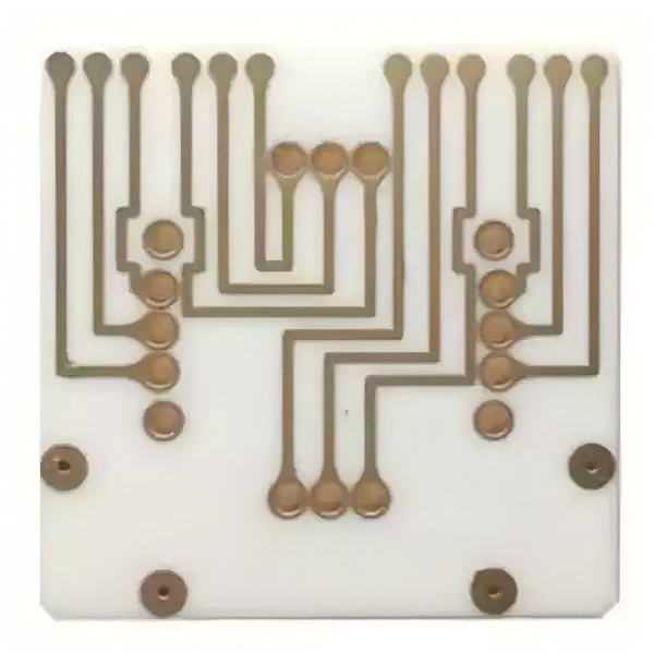
Ceramic Substrate + Thick Copper: Not Just Materials, but a Thermal Strategy
When engineers transition to a high thermal conductivity ceramic PCB, they are not simply switching materials. They are redefining how heat flows through the system.
Ceramic substrates such as AlN and Si₃N₄ provide a fundamentally different thermal behaviour compared to conventional structures. Heat is no longer trapped or forced to navigate complex paths. Instead, it moves quickly and directly through the substrate, reducing internal thermal resistance.
However, in real designs, vertical heat conduction alone is not enough. High-power systems rarely generate heat evenly. Switching devices, power traces, and driver circuits all create uneven thermal profiles. Without proper redistribution, hotspots will still form.
This is why thick copper plays a critical role.
In a well-designed high thermal conductivity ceramic PCB, copper layers act as controlled heat spreaders rather than simple conductors. Their thickness and geometry are carefully adjusted to balance electrical and thermal performance.
A practical design typically needs to handle three constraints at the same time:
🟠 Current density must remain low enough to avoid additional heat generation
🟠 Parasitic inductance must be controlled for switching stability
🟠 Heat must spread laterally before it concentrates
When these factors are aligned, the PCB behaves as a unified electro-thermal system. Temperature gradients are reduced, and thermal stress is distributed more evenly across the structure.
This is the difference between a board that “survives” high power and one that can operate reliably over thousands of hours.
Manufacturing Capability: Where Good Designs Either Succeed or Fail
Even the most carefully engineered high thermal conductivity ceramic PCB can fall short if the manufacturing process is not tightly controlled.
This is where the role of an experienced PCB fabrication manufacturer becomes decisive.
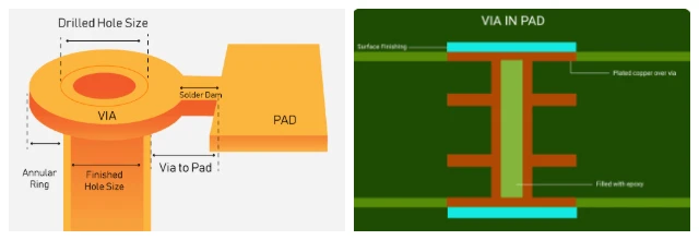
Ceramic PCB structures are far less forgiving than standard boards. The interface between copper and ceramic must be uniform and stable. Any microscopic void, weak bonding area, or uneven metallization can introduce localised thermal resistance.
These defects are not always visible during initial testing. Instead, they tend to evolve under long-term thermal cycling, eventually leading to failure.
A capable PCB fabrication manufacturer focuses on controlling these risks at the process level. That includes lamination profiles, metallization consistency, and interface bonding quality. The goal is to eliminate weak points before they ever reach the field.
Multi-layer ceramic PCBs introduce an additional layer of complexity. Each layer responds differently to temperature changes, and internal stress can accumulate if the structure is not properly balanced. Over time, this can lead to cracking or delamination.
Manufacturers with real experience in high thermal conductivity ceramic PCB production address this through controlled stacking strategies and stress management techniques. These are not visible features, but they directly impact long-term reliability.
In real product development, this level of control also affects project timelines. Stable manufacturing reduces iteration cycles, allowing engineering teams to validate designs faster and move into production with confidence.
Proven Performance: What Engineers Actually Gain
The advantages of a high thermal conductivity ceramic PCB become much clearer when evaluated under real operating conditions rather than theoretical comparisons.
Below is a summary of typical performance characteristics observed in high-power applications:
| Parameter | Typical Value | Practical Impact |
|---|
| Thermal Resistance | < 1°C/W | Faster heat transfer, lower junction temperature |
| Substrate Thermal Conductivity | 170–230 W/m·K | Efficient vertical heat conduction |
| Continuous High-Temp Operation | 150°C for 500+ hours | Stable long-term performance |
| Thermal Cycling Reliability | >2000 cycles (-40°C to 150°C) | Reduced risk of cracking or delamination |
| Copper Thickness Range | 100–300 µm | Supports high current and improves heat spreading |
| Hotspot Reduction | 30%–50% improvement | Prevents localized overheating |
| Electrical Loss Reduction | 15%–25% | Less self-heating, higher efficiency |
What these numbers show is not just better thermal performance, but a more stable operating environment for the entire system.
In practice, a well-designed high thermal conductivity ceramic PCB allows power devices to run at lower and more uniform temperatures. This reduces thermal stress on solder joints and interfaces, which are often the first points of failure.
It also helps maintain electrical consistency. As temperature variation decreases, so does parameter drift, leading to more predictable system behaviour over time.
Real Impact in High-Power Applications
The benefits of a high thermal conductivity ceramic PCB are most visible in systems that operate under continuous or high-load conditions.
In power conversion systems, improved heat transfer allows designers to increase power density without exceeding thermal limits. Instead of relying on oversized cooling solutions, the PCB itself becomes part of the thermal management strategy.
In automotive applications, especially in EV inverters, long-term reliability is critical. Components are expected to operate under wide temperature ranges and repeated thermal cycling. A stable thermal structure directly reduces failure risk over the product lifecycle.
In industrial environments, where downtime is costly, consistent performance matters more than peak performance. Systems built on high thermal conductivity ceramic PCB technology maintain their characteristics over time, reducing maintenance and replacement frequency.
Across these scenarios, the pattern is consistent: better thermal control leads to better reliability, not just better performance.
A Structural Solution to a Thermal Problem
Thermal management in high-power electronics cannot be treated as an afterthought. As power density continues to increase, the limitations of conventional approaches become more apparent.
A high thermal conductivity ceramic PCB offers a fundamentally different solution. By combining high-performance ceramic substrates, optimised thick copper structures, and controlled manufacturing processes, it creates a low-resistance thermal path directly within the board.
Just as importantly, working with a capable PCB fabrication manufacturer ensures that these design advantages are preserved in production, not lost due to process variation.
For engineers and product managers, the shift toward ceramic PCB technology is not just about improving heat dissipation. It is about building systems that remain stable, predictable, and reliable over the long term.
In high-power applications, that difference is often what separates a design that works in the lab from one that performs in the real world.
About the auther:

Sonic Yang
As a major of Electronics and Mechanical Automation, Sonic has been engaged in PCB design, R&D, manufacturing of eletronics for around 22 years, as engineering director and coordinates with supply chain(components&CNC parts), providing professional supports and consults for global customers.
 en
en


 WhatsApp