I. What are Thermal Vias?
Thermal vias are clusters of vias specifically designed to rapidly conduct heat from one layer of a PCB (usually the top or inner layer where heat-generating components are located) to other layers (especially the bottom copper layer or inner copper layer). They are not heat sinks but rather efficient for heat conduction, diffusing heat from the "heat source" to a larger copper area on the PCB, where it is dissipated through convection and radiation.
II. Core Functions and Purposes
1. Reduce Thermal Resistance: Chips (especially with pads on the bottom, such as QFN, DFN, and BGA) have high thermal resistance to the air. Via arrays conduct heat to a large area of copper foil on the bottom or inner layers of the PCB, reducing the total thermal resistance significantly from the joints to the environment.
2. Heat Distribution and Dissipation: Dissipating heat from a point(heat source) to a larger area rapidly, prevents localized overheating.
3. Connection to Thermal Structures: Conducting heat to the back of the PCB, which also support to install external heatsinks, dissipate heat through casing, or direct exposure to airflow.
III. Key Design Considerations
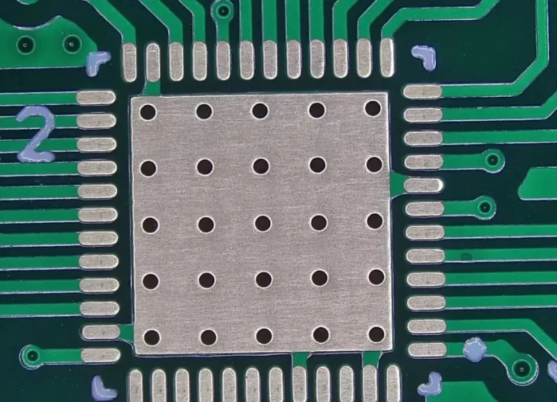
1. Layout and Array
● Located Below Heat Source: Typically, place vias directly below the thermal pads of heat-generating devices (such as chips).
● Array Formation: Utilizing a tightly packed array of vias, rather than individual vias. Commonly array like matrix or quincunx formation, to maximize heat conduction area.
2. Via Parameters
● Hole Diameter: Typically small via diameters (e.g., 0.3mm - 0.5mm). Smaller diameters allow for more vias within a limited area, increasing the overall heat conduction cross-sectional area. However, the PCB manufacturer's process capabilities (minimum hole diameter) must be considered.
● Copper Thickness on Hole Wall: Maximize the copper thickness of the hole walls. Specify "thick copper fill" or "thicker hole wall plating" (e.g., 1 ounce or more) to the PCB manufacturer. This is one of the most effective ways to improve thermal conductivity.
● Spacing: The center-to-center pitch between vias is generally about twice the hole diameter to ensure sufficient copper rings and avoid hole breakage during drilling. Too dense a pitch can lead to signal integrity issues (creating resonant cavities) or manufacturing difficulties.
3. Connecting Layers and Solder Mask
● Connect all possible large copper layers: Ideally, thermal vias should connect to all internal power/ground planes and the bottom copper foil. This is equivalent to connecting the heat source to a large "thermal mass."
● Solder Mask Openings: On the back (bottom layer) of the PCB, in the area corresponding to the via, be sure to create solder mask openings (i.e., prevent solder mask from covering the copper and vias). This allows:
* Dissipate heat directly to the air.
* Easy to solder additional heatsinks or metal blocks.
* Thermal grease can be applied if needed.
4. Connection to Inner Copper Layers
● Vias should be fully connected to the inner copper layers (flood connect), not using thermal relief cross connections. For heat dissipation, we need the lowest thermal resistance path.

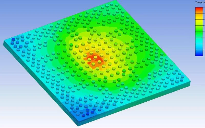
IV. Considerations in Thermal Simulation
When performing thermal simulations in EDA software (such as ANSYS Icepak, Simcenter Flotherm, Altium Sim, etc.):
● The via array needs to be modeled as an equivalent thermally conductive block, with an equivalent thermal conductivity that much higher than ordinary FR-4 material.
● The model needs to consider factors such as via wall copper thickness, filler (air or resin), and packing density to calculate the equivalent thermal conductivity.
● The main purpose of the simulation is to evaluate the impact of different via designs on chip junction temperature and PCB surface temperature distribution.
V. Advanced Techniques and Variations
1. Filled Vias:
● Conductive Filler: Filled with copper paste or conductive epoxy resin, offering excellent thermal conductivity but at high cost.
● Non-Conductive Filler: Filled with resin and then surface plated (VIPPO). It's main purpose is to prevent solder paste loss during front-side chip mounting, and it also provides some improvement in thermal conductivity (better than air).
● Thermally Conductive Epoxy Resin Filler: Filled with a special high thermal conductivity insulating material, improving thermal conductivity while ensuring electrical isolation.
2. Applicable to high-power devices:
Thermal vias are essential for MOSFETs, high-current DC-DC converters, etc. They are typically placed over a large area beneath the device.
3. Precautions:
● Signal integrity: Dense array of vias may disrupt the reference plane which beneath high-speed signal lines (especially microwave and RF), creating discontinuities. Discreet evaluation is required.
● Soldering issues: If vias are directly on surface mount pads (especially pads for small chips), proper solder mask plugging is essential to prevent solder paste loss during reflow soldering, leading to cold solder joints.
VI. Summary of Design
1. Identify heat sources: Locate the main heat-generating components on the PCB.
2. Plan the paths for heat dissipation: Determine which layer (usually the back) to conduct heat.
3. Place via array: Place dense, small-diameter vias under the device's thermal pads.
4. Set via properties: Specify thickened via wall copper, connecting to all relevant copper layers.
5. Solder mask: Ensure solder mask openings in the back heat dissipation areas.
6. DFM Inspection: Communicate with the PCB manufacturer to confirm the feasibility and cost of processes such as hole diameter, copper thickness, and via filling.
7. Perform Thermal Simulation: Verify the design effectiveness.
In summary, PCB thermal vias are a low-cost, high-efficiency method for built-in heat dissipation. The core purpose is "utilizing the entire copper layer of the PCB as a heat sink." Design of vias is key to the successful thermal management, especially in power electronics and compact devices.
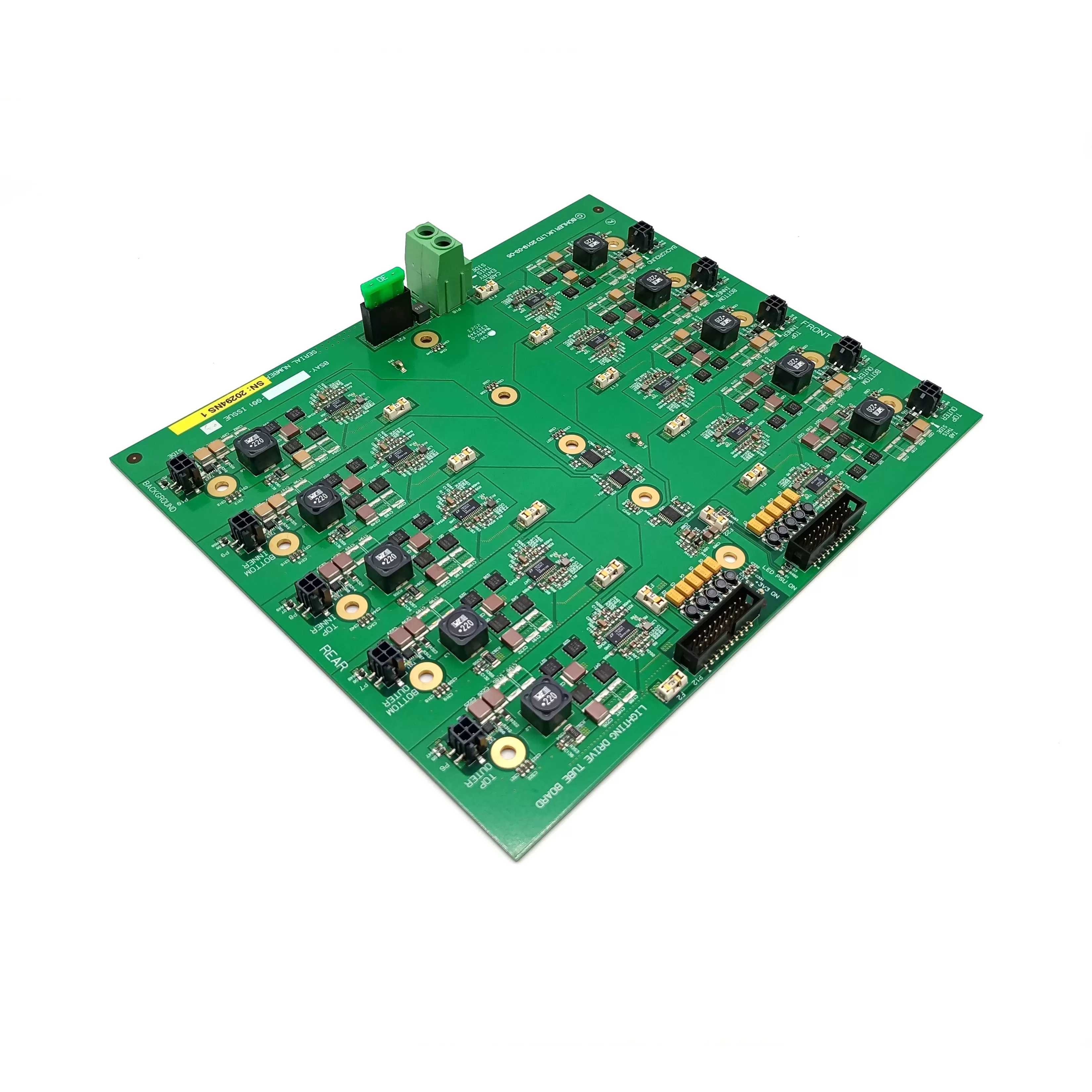
Benlida has been manufacturing PCBs and PCBAs for 14 years, it has established a production system: from advanced equipment to engineering team, from process control to strong supply chain. We have very mature manufacturing processes for PCB thermal vias, if you need custom PCB, please contact Benlida!
 en
en


 WhatsApp