When PCB Supply Becomes the Bottleneck
If you’ve been involved in hardware projects long enough, you’ve probably seen this scenario play out more than once.
The PCB arrives later than promised. The first batch passes basic inspection, but issues start showing up during assembly. Engineering blames fabrication, assembly points to design files, and procurement is stuck coordinating between three different vendors—none of whom take full ownership.
On paper, everything looked fine. In reality, the project timeline slips.
This is why more teams—especially in industrial control, medical electronics, and automotive systems—are rethinking how they choose suppliers. Instead of splitting fabrication, assembly, and sourcing across multiple vendors, they’re moving toward partners who can handle both industrial PCB manufacturing and a complete PCB solution under one roof.
Not because it sounds better, but because it works better when timelines are tight, and failure isn’t an option.
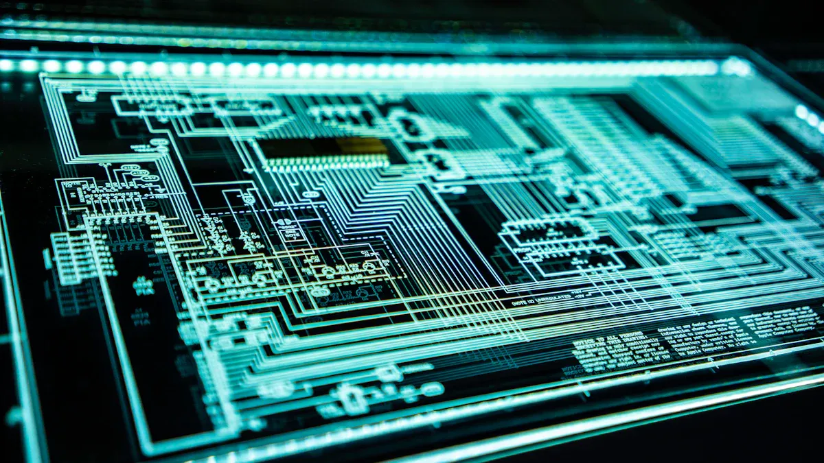
Industrial PCB Manufacturing: What Actually Matters on the Shop Floor
Most suppliers will say they can build multi-layer boards or handle HDI. The difference shows up when those boards go into real applications—running 24/7, exposed to noise, heat, and mechanical stress.
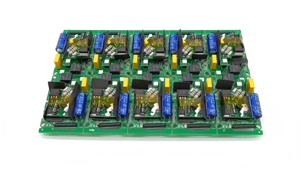
Multi-Layer PCBs: It’s Not About Layer Count
Yes, 1–36 layer capability sounds impressive. But what engineers really care about is consistency across those layers.
In one industrial control project we supported, the customer was dealing with intermittent signal instability on an 18-layer board. The design itself was solid. The issue turned out to be a variation in dielectric thickness between batches, which caused impedance drift.
After switching to a more controlled lamination process, the problem disappeared—no design change needed.
What makes the difference in multi-layer manufacturing:
- Stable lamination cycles, not just stacking capability
- Tight control of prepreg flow and dielectric thickness
- Accurate layer-to-layer registration
- Repeatability across batches, not just within a single run
For systems that rely on precise signal timing, these details are not optional.
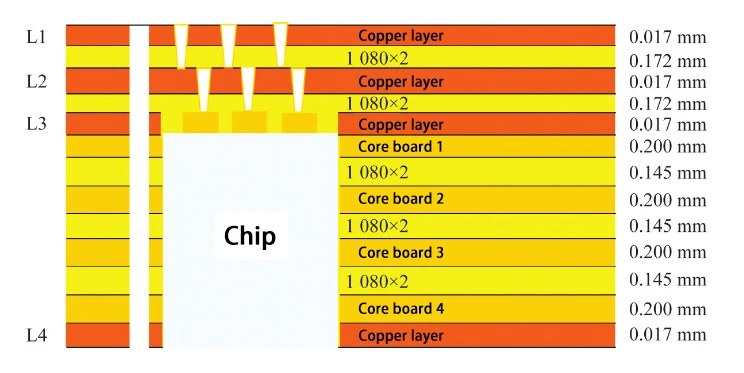
HDI: Where Process Control Gets Tested
HDI boards push manufacturing into a different level of precision. Microvias, blind vias, stacked structures—these are not forgiving processes.
We’ve seen cases where via reliability becomes the hidden failure point. Boards pass initial tests, but after thermal cycling, microvia cracks start to appear.
A mature HDI process typically shows in:
- Consistent laser drilling quality (no irregular via walls)
- Reliable via filling without voids
- Controlled plating thickness inside microvias
- Proven performance under thermal stress
In medical electronics, especially portable or implantable devices, HDI is often unavoidable. But it only works when the process behind it is stable.
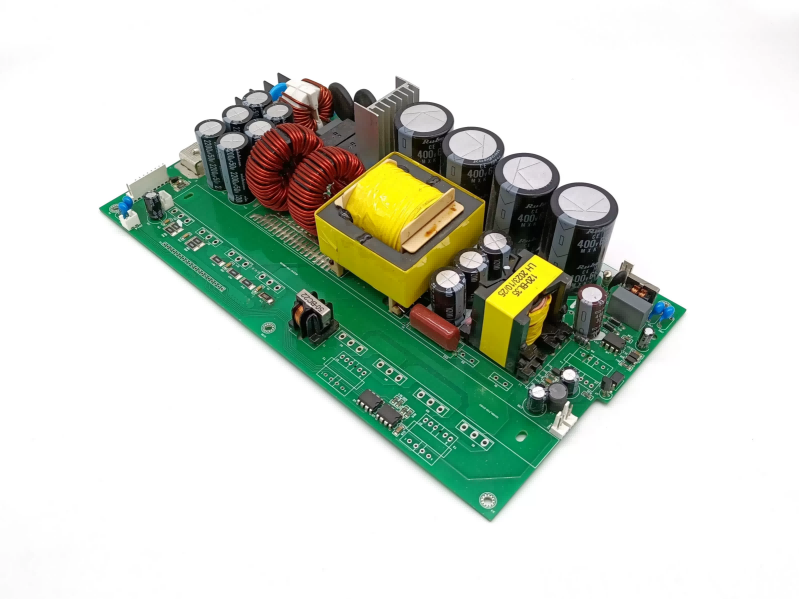
High-Frequency Materials: Where Theory Meets Reality
High-frequency PCB design looks clean in simulation. In production, material handling becomes critical.
One RF module project we worked on used a hybrid stack-up with PTFE and FR4. Early prototypes from another supplier showed higher-than-expected signal loss. The root cause wasn’t the design—it was inconsistent bonding between different material layers.
Once the stack-up process was adjusted and material handling standardized, insertion loss dropped back into the expected range.
What matters in high-frequency boards:
- Experience with mixed-material stack-ups
- Controlled lamination parameters for PTFE-based substrates
- Clean drilling and minimal resin smear
- Reliable impedance matching between simulation and production
At high frequencies, small deviations show up quickly.
Impedance Control: Where Tolerance Becomes Visible
Many suppliers claim impedance control. The real question is: how tight, and how consistent?
In high-speed communication boards, even a ±10% variation can start causing reflections and signal degradation. For some designs, engineers are expecting ±5% or tighter.
What experienced teams look for:
- Pre-production stack-up validation, not guesswork
- Measured impedance reports for each batch
- Alignment between design simulation and actual production results
When impedance is off, the system may still work—but not reliably, and not across all conditions.
Where These Details Show Up
You don’t notice these differences in a lab demo. You notice them when:
- An industrial controller runs continuously and starts showing random faults
- A medical device fails validation under repeated stress testing
- An automotive module behaves inconsistently under temperature variation
That’s where manufacturing quality stops being a spec sheet and becomes a real factor.
One-Stop PCB Solution: Fewer Handovers, Fewer Problems
Separating PCB fabrication, assembly, and sourcing might seem flexible. In practice, it often creates more problems than it solves.
Every handoff is a potential failure point.
A Real Example: When Coordination Becomes the Problem
One customer in the industrial automation sector came to us after struggling with a delayed project.
Their setup was typical:
- PCB fabrication from one vendor
- SMT assembly from another
- Components sourced separately
The issue wasn’t a single major failure. It was a series of small mismatches:
- Slight PCB warpage affecting SMT yield
- Component substitutions not fully aligned with the assembly process
- Delays in feedback between vendors
After moving to an integrated PCB solution, the same product went through:
- Unified DFM review before production
- Aligned PCB and assembly process parameters
- Centralized component sourcing
The result:
- Assembly yield improved noticeably
- Rework dropped significantly
- Overall project cycle shortened by nearly 40%
No redesign. Just better coordination.
Why Integration Changes the Outcome
When PCB manufacturing and assembly are handled together, decisions are no longer isolated.
For example:
- Pad design is reviewed with SMT placement in mind
- PCB warpage is controlled based on assembly requirements
- Component sourcing considers real assembly compatibility
Instead of reacting to problems, the process avoids them earlier.
Communication Becomes Simpler—and Faster
From a project management perspective, the difference is obvious:
- One point of contact instead of multiple vendors
- Faster response to engineering changes
- Clear responsibility when issues arise
For procurement teams, this reduces uncertainty.
For engineers, it reduces iteration cycles.
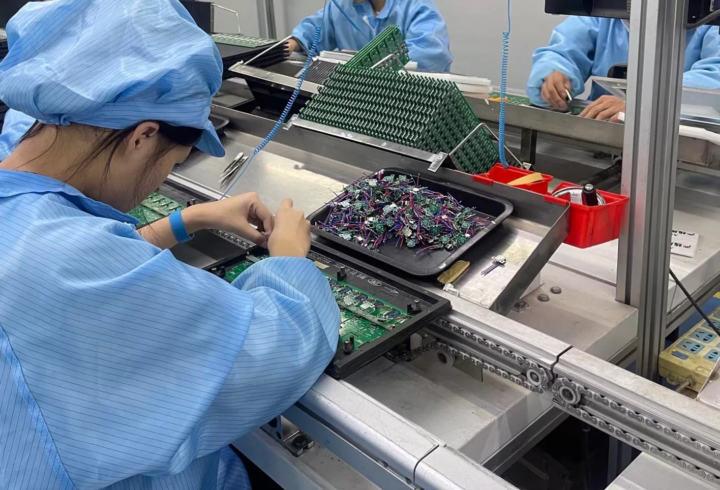
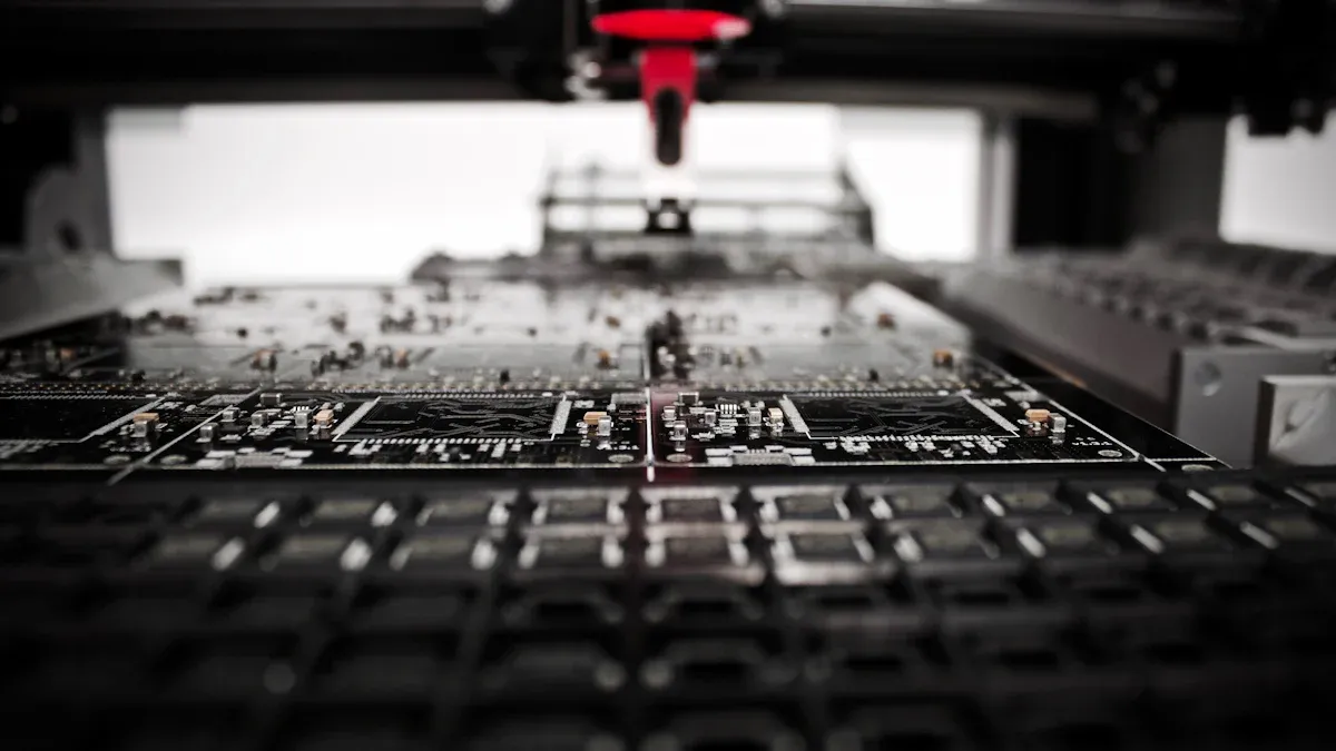
Testing Is More Meaningful When It’s Integrated
AOI, X-ray, ICT, FCT—these are standard terms. What matters is how they are used.
In a fragmented setup, testing is often disconnected:
- PCB is checked separately
- The assembly is inspected later
- Functional testing may come last
In an integrated setup, testing becomes part of the flow:
- AOI catches placement issues early in SMT
- X-ray verifies hidden solder joints before failure shows up in use
- ICT ensures electrical integrity before functional testing
- FCT simulates real operating conditions
We’ve seen cases where adding X-ray inspection for BGA components alone reduced hidden defect-related failures by a significant margin in early production runs.
Testing is not just about catching defects—it’s about catching them at the right stage.
Speed and Capacity: What They Actually Change for You
Everyone talks about fast turnaround. The real question is how that speed impacts your project.
Prototyping Speed: Where Time Is Won or Lost
For most engineering teams, the biggest pressure is during the prototype stage.
A typical scenario:
- Prototype reveals issues
- Design needs adjustment
- The next iteration is required quickly
If each cycle takes 10–14 days, the timeline stretches quickly.
If it takes 3–7 days, the same project moves much faster.
The difference is not just days saved—it’s how many iterations you can complete before your deadline.
Scaling to Production Without Disruption
Moving from prototype to mass production is where many projects slow down.
What helps:
- Sufficient PCB production capacity (e.g., up to 50,000㎡ per month)
- Multiple SMT lines to handle parallel orders
- Process consistency between small batch and large batch production
Without this, you may get a good prototype—but struggle in volume.
SMT Throughput and Stability
SMT capacity is not just about speed, but also about stability under load.
In real production environments:
- Multiple SMT lines allow better scheduling flexibility
- Automated inspection within the line reduces bottlenecks
- Stable equipment performance ensures consistent output
This becomes critical when deadlines are tight and volumes increase.
What Customers Actually Gain
From the customer side, these capabilities translate into:
- Faster validation cycles during development
- More predictable delivery timelines
- Reduced need for buffer stock
- Better ability to respond to market demand
In short, fewer surprises.
What a Reliable Partner Looks Like in Practice
At a glance, many PCB suppliers look similar. The difference becomes clear only when a project is under pressure.
A partner with strong industrial PCB manufacturing capability and a complete PCB solution doesn’t just deliver boards—they remove friction from the entire process.
That shows up as:
- Fewer unexpected issues during assembly
- More stable performance in real applications
- Shorter and more predictable project timelines
- Less time spent coordinating, more time spent building
For engineering teams, it means fewer late-night debugging sessions.
For procurement, it means fewer escalations.
For the business, it means projects that move forward as planned.
Ready to Move Faster with Fewer Risks?
If your current setup is causing delays, quality concerns, or coordination headaches, it may be time to rethink your approach.
Work with a partner who can support both industrial PCB manufacturing and a complete PCB solution—from fabrication to assembly to testing.
Get a Quote or Contact US to discuss your project.
About the auther:

Sonic Yang
As a major of Electronics and Mechanical Automation, Sonic has been engaged in PCB design, R&D, manufacturing of eletronics for around 22 years, as engineering director and coordinates with supply chain(components&CNC parts), providing professional supports and consults for global customers.
 en
en


 WhatsApp