Why Correct Design Still Fails in Production
In industrial control systems, automotive electronics, and smart appliance interfaces, switch-related PCB failures rarely come from obvious schematic mistakes. More often, they appear only under real operating conditions—load stress, vibration, thermal cycling, or long-term switching cycles.
This is where many engineering teams run into a practical gap: a design that looks solid on paper and even passes prototype validation can still fail in mass production or field use.
In real engineering terms, PCB Assembly for Switch applications is not just component placement. It is the interaction of electrical design, mechanical stress behaviour, and manufacturing stability under repeated real-world conditions.
Most failures are not single-point defects. They are system-level mismatches that only become visible after deployment.
Soldering and Interconnect Reliability Problems
Solder joints are one of the most common weak points in switch PCB systems, especially where repeated actuation or vibration is involved.
Cold solder joints and hidden intermittency
Cold joints may pass visual inspection but fail under thermal or mechanical stress. They often show up as intermittent open circuits after extended operation.
Vibration-induced micro-cracking
In industrial environments, vibration slowly introduces microfractures in solder joints. These defects are especially critical near heavier components and through-hole terminals.
SMT and THT selection imbalance
Over-reliance on SMT for mechanically stressed areas is a recurring issue in PCB Assembly for Switch designs. While SMT improves efficiency, THT often provides better mechanical anchoring.
| Issue Type | Typical Cause | Field Impact |
|---|
| Cold solder joint | Insufficient heat transfer | Intermittent signal loss |
| Vibration cracking | Mechanical stress cycles | Long-term open circuit |
| SMT overuse | Design for cost efficiency | Reduced mechanical stability |
A balanced hybrid approach is often required rather than a purely SMT-driven design.

Design Related Functional Issues
Many failures are incorrectly attributed to manufacturing when the root cause is actually design-related.
Trace width and thermal stress
Undersized power traces can gradually overheat under repeated switching loads, leading to resistance drift and eventual failure.
Grounding structure weaknesses
Poor grounding design introduces noise coupling between switch signals and control logic, resulting in unstable triggering behaviour.
EMI sensitivity in switching zones
Without proper isolation, electromagnetic interference can cause false triggering or missed signals in high-density switch layouts.
A key engineering reality in PCB Assembly for Switch systems is that design decisions define reliability more strongly than assembly precision in many cases.
Material and Environmental Stress Factors
Switch PCBs behave more like electro-mechanical systems than static circuits.
Thermal and humidity drift
Standard FR4 materials can experience dielectric changes under high humidity or temperature cycling, affecting signal stability.
Copper thickness limitations
Insufficient copper thickness increases resistance over time, especially in power-switch circuits with repeated load cycling.
Lack of protective coating
Without conformal coating, moisture and contaminants gradually degrade exposed copper and solder joints.
Vibration fatigue
Mechanical vibration continuously stresses both components and solder joints, accelerating long-term degradation.
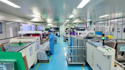
Assembly and Production Consistency Issues
Even a well-designed PCB can fail if manufacturing consistency is not tightly controlled.
SMT placement variation
Small deviations in component placement can affect signal integrity in sensitive switch detection circuits.
Reflow profile instability
Incorrect temperature curves can weaken solder joints or introduce internal stress that reduces lifespan.
Batch variation in production
Differences in solder paste, component sourcing, or machine calibration can create performance inconsistencies between batches.
Insufficient test coverage
Many lines rely only on AOI and ICT testing, which cannot simulate real-world mechanical or thermal stress conditions.
How to Avoid These Problems
Reliability in switch PCB systems is not achieved by fixing defects later. It is built into the process from the beginning.
Engineering controls that matter most
●Early integration of DFM and DFA
●Proper segmentation of power and signal layers
●Controlled solder profile optimisation
●Environmental stress validation before mass production
Key validation methods used in industrial applications
| Test Method | Condition | What it reveals |
|---|
| Thermal cycling | 500–1000 cycles | Solder fatigue and material drift |
| Vibration testing | 10–2000 Hz range | Mechanical joint stability |
| Power load testing | Continuous switching | Thermal resistance growth |
| Pilot production run | Small batch validation | Manufacturing variability |
These steps are critical in any serious PCB Assembly for a switch project, especially for industrial or automotive use cases.
Failures in switch PCB systems are rarely random. They are predictable engineering outcomes caused by mismatches between design assumptions, material behaviour, and manufacturing reality.
Most issues in PCB Assembly for Switch do not originate from a single defect but from accumulated small compromises across design, materials, and production processes.
In practical engineering terms:
Reliable switch PCB performance is not validated at the end of production. It is guaranteed at the design stage and confirmed through disciplined manufacturing control.
About the auther:

Sonic Yang
As a major of Electronics and Mechanical Automation, Sonic has been engaged in PCB design, R&D, manufacturing of eletronics for around 22 years, as engineering director and coordinates with supply chain(components&CNC parts), providing professional supports and consults for global customers.
 en
en


 WhatsApp