The PCBA(Printed Circuit Board Assembly) of Bitcoin miner (ASIC miner) is the core and determines cost. It's design and manufacturing requirements directly impact the miner's hashrate, energy efficiency and reliability. This article is a detailed analysis of structural features, key manufacturing points and critical process requirements for miner's PCBA.
I. Core Structural Features of PCBAs
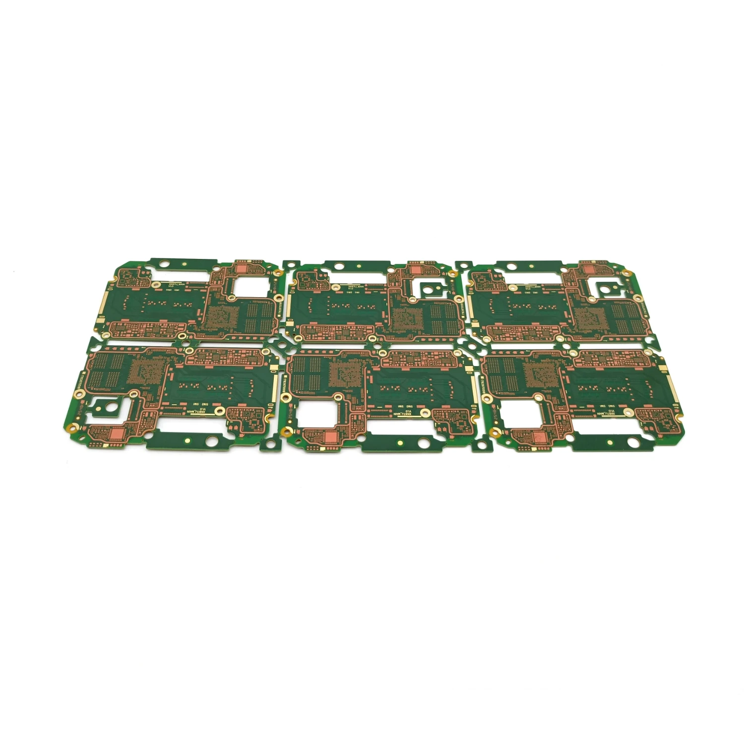
PCBA of every Bitcoin miner is not just an ordinary PCB/printed circuit board, but a computing matrix with ultra-high density, ultra-high power consumption, and ultra-high heat load.
1. Core Component Array:
● ASIC Chips: Dozens even hundreds of dedicated mining chips are the absolute core of the PCBA. They are arranged in a high-density array.
● Hash Board: Typically, multiple ASIC chips and their associated circuitry form a "hash board." A single miner operates with multiple hash boards in parallel.
2. Ultra-High Power Supply Network:
● Voltage Conversion Stages: The 12V input from the miner's power supply undergoes multi-layer DC-DC conversion (e.g., first to the 0.6-0.8V core voltage) to power the ASIC chip. Every 1% loss in conversion efficiency results in significant heat generation and electricity costs.
● High Current Channels: A single hash board can consume several kilowatts, drawing extremely high currents. The PCB needs to be designed with very thick copper layers (e.g., 6OZ or even more) or embedded copper strips as power channels.
3. Dense Heat Dissipation Interface:
● The bottom of the ASIC chip typically attached to the heatsink or liquid cooling system directly. Numerous heat dissipation vias are present on the corresponding locations on the PCB, to transfer heat from the top of the chip to the bottom heatsink for heat dissipation.
4. Control and Communication:
● Compared to the hash power section, the control section is relatively simple. It typically includes a control MCU, a network interface (e.g., Ethernet), a management interface, and a small amount of memory.
II. Key Considerations for PCBA: Design to Manufacturing
1. Key Considerations in PCB Design and Manufacturing
● Number of Layers and Materials: Typically, high Tg (glass transition temperature) PCB board with 8 or even more layers are commonly applied, such as FR-4 Tg170. High-end miners use boards with even better thermal conductivity (such as those containing ceramic materials).
● Copper Thickness is Crucial: To handle hundreds of amperes of current, power and GND layers use extremely thick copper foil, such as 3OZ, 4OZ or even 6OZ. This presents significant challenges to etching and lamination processes for PCB manufacturer.
● Thermal Via Design: A dense array of thermally conductive vias filled with thermally conductive material is designed on the bottom of the ASIC chip. These vias require excellent electroplating or plugging processes, to ensure efficient heat conduction and surface smoothness, facilitating heatsink installation.
● Power Integrity: Due to the extremely high instantaneous current, the decoupling capacitor network and power plane must be carefully designed to suppress voltage fluctuations and noise, ensuring stable operation of the ASIC chip.
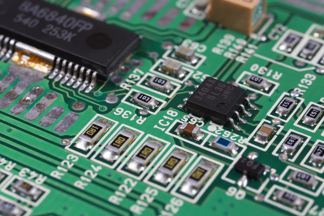
2. Key Points of SMT (Surface Mount Technology) Assembly Process
● High-Density Assembly: ASIC chips are typically packaged in BGA or QFN packages, with numerous and densely packed pins. This requires high-precision SMT machines and strict process control.
● Large Component and Reflow Soldering: PCB carriess both tiny resistors & capacitors(package 0603, 0402, 0201) and large components such as power inductors and MOSFETs&IGBT. The reflow soldering temperature profile must be carefully considered to prevent large components absorbing too much heat and meanwhile causing cold soldering on smaller components, or overheating and damaging smaller components.
● Bottom Pad and Heat Dissipation: ASIC chips usually have a large pad on the bottom for thermal dissipation, which must be well soldered to the thermal pad on the PCB. This requires the PCB pad to be designed with sufficient thermal vias, and the stencil openings must ensure sufficient volume of solder paste.
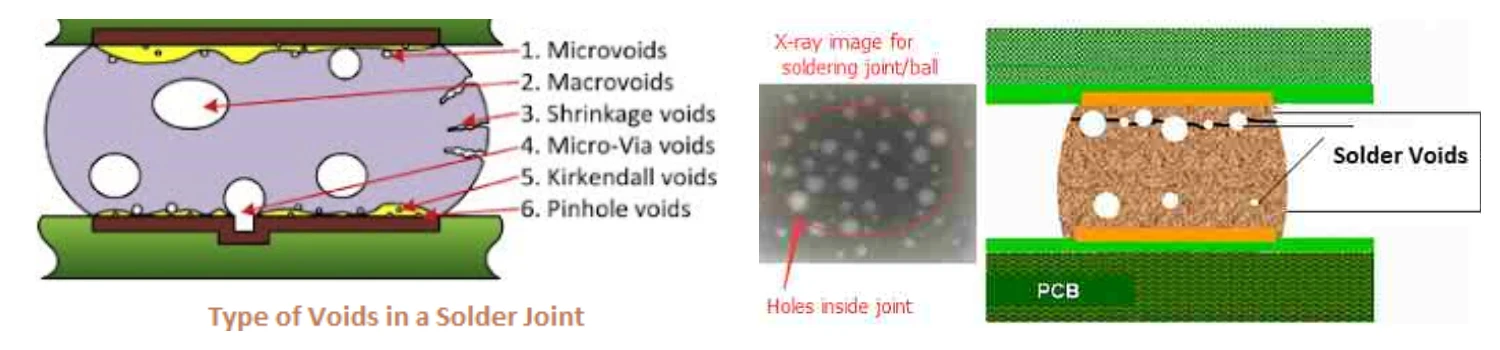
● X-Ray Inspection is mandatory: Since BGA solder joints are not visible, X-ray inspection is 100% mandatory step to check defects, such as solder bubbles, short, and misalignment of solder pads.
3. THT and Process Key Points
● High Current Connectors: Connectors between power input terminals and the computing board need to withstand high currents, typically using robust crimping or soldering connections.
● Conformal Coating: In non-heat dissipation areas, conformal coating may be applied to prevent corrosion and short circuits in humid, dusty environments. This coating must be avoided along heat dissipation paths and connectors.
● Stress Relief: Miner will experience vibration and thermal expansion/contraction during transportation and operation. Large components (such as inductors) require adhesive reinforcement to prevent solder joint cracking from fatigue.
III. Core Process Challenges and Considerations
1. Thermal Management is the Primary Challenge:
● PCB as a Heat Conduction Path: The PCB itself is a part of the heat dissipation system. Thick copper, thermal vias, and high thermal conductivity substrates are all used to reduce thermal resistance.
● Solder Void Rate Control: Voids in the bottom pads of ASIC chips severely impede heat conduction. The void rate must be controlled to an extremely low level (e.g., <15%) through optimized stencil design, solder paste selection, and reflow profiles.
● Flatness Requirements: The warpage of the entire hash board must be extremely small to ensure uniform contact between all ASIC chips and the heatsink, preventing localized overheating.
2. Reliability Issues Due to High Current:
● Electromigration: Under prolonged high current operation, metal atoms within the copper conductors gradually migrate, causing the conductors to thin or even break. This necessitates designing sufficient width/copper thickness of traces and choose high-quality PCB manufacturing.
● Thermal Cycling Fatigue: Miners operate 24/7, constantly experiencing temperature cycles due to start-stop cycles and load variations, posing a severe challenge to BGA solder joints and the chip packaging itself. Optimizing solder ball alloys and using underfill processes are necessary to extend lifespan.
3. Complexity of Testing and Programming:
● Functional Testing: Basic functional testing is required for each ASIC chip, calculating its hashrate and power consumption, and classifying it (Binning). Efficient test fixtures and software are very important.
● Aging Testing: Long-term power-on aging at high temperatures is typically required to eliminate early-failure PCBAs and ensure the stability of the miners before they leave the factory.
4. The Ultimate Balance Between Cost and Efficiency:
● Miner is a brutally competitive business, every improvement in efficiency (J/TH) or reduction in cost is crucial. PCBA design must achieve an optimal balance between material costs (e.g., gold/copper materials), process costs, and final performance/reliability.
Summary:
PCBA manufacturing for Bitcoin miner represents the pinnacle of process complexity and reliability requirements in the consumer electronics field. It integrates:
● Server-level: power density and heat dissipation challenges.
● Communication equipment-level: high-speed signal integrity requirements (internal clock network).
● Industrial control-level: 24/7 operational reliability requirements.
● Extreme cost control in cost-sensitive consumer electronics.
It's core processes revolve three pillars: "heat dissipation," "power supply," and "reliability." Neglecting any of these could lead to a decrease in overall computing power, a surge in power consumption, or large-scale failures, reducing competitive advantage in the mining industry.
Benlida has been manufacturing PCBs and PCBAs for 14 years and has established a complete production system: from advanced equipment to process engineers, from process control to a strong supply chain. We have mature experience in the production and assembly of miner PCBAs. If you need to customize PCBAs for Bitcoin miners, please feel free to contact Benlida to explore more!
 en
en

 WhatsApp