The root causes of components cracking come from the mechanical or thermal stress: during manufacturing, assembly, or working status, and the stress exceeds the mechanical strength of it's material (usually ceramic, silicon, or plastic encapsulation). This is a typical issue of process reliability.
The core reason is "stress concentration" and the specific causes can be categorized as following:
I. Cracks caused by thermal stress (one of the most common causes)
1. Reflow soldering temperature shock
● Cause: Mismatch in the coefficients of thermal expansion between the components and the solder joints, or between the component and the PCB substrate. During the rapid heating and cooling process of reflow soldering, the contraction/expansion of different parts is inconsistent, generating internal shear forces.
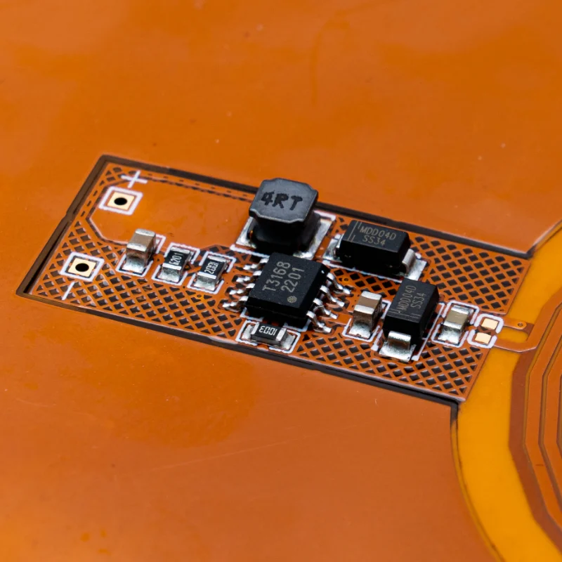
● Typical characteristics: Cracks often originate at the junction of the solder joint and the components, or in the center of the bottom of the components. Commonly happen on MLCCs (multilayer ceramic capacitors), thick-film resistors, and large-size ceramic packaged components.
2. Secondary Overheating During Wave Soldering
● Cause: On PCBs which have undergone SMT assembly, the components exposed to high-temperature solder for an extended period during wave soldering, leading to accumulated thermal stress.
● Typical Characteristics: Occurs on PCBs when require mixed assembly processes; cracked components are often assembled by SMT, located on the surface(bottom) for wave soldering.
3. Improper Rework Operations
● Cause: Localized high-temperature heating (hot air gun) and rapid cooling create a large local thermal gradient.
● Typical Characteristics: Random cracking occurs in components around the rework area.
II. Cracks Caused by Mechanical Stress
1. Separation Stress
● Cause: Bending or vibration stress generated during mechanical cutting (V-cut, or other separator) or manual dividing may transfer to brittle components directly.
Typical Characteristics: Cracked components are near the PCB edge or V-cut groove. MLCCs are a particularly vulnerable.
2. PCB Bending or Deformation
● Assembly Process: Overtightening of screws, bending of the board during installation in the fixture, and connector insertion/extraction forces causing board deformation.
● Design Issues: Insufficient PCB strength, causing bending under it's own weight or external forces.
● Typical characteristics: Cracks may appear on large components near the center of the PCB or fixed points.
3. Test Probes or External Impacts
● Causes: Excessive pressure applied by probes during in-circuit testing or functional testing; drops or collisions during production handling.
● Typical characteristics: Localized damage, possibly with visible external impact points.
III. Component and Process Design Matching Issues
1. Inappropriate Pad Design
● Causes: Pads that are too large or too small result in poor solder joint shape after reflow, creating additional tensile or compressive stress on the components.
● Typical characteristics: One end of the component is pulled up (tombstone effect), or the bottom is excessively compressed.
2. Component Selection and Layout Issues
● Cause: Oversized (e.g., 1210 and larger) MLCCs or ceramic-packaged components were used in stress-sensitive areas (e.g., near board edges, screw holes, bends).
● Typical Characteristics: Batch problems with the same specifications in specific locations.
3. Stencil Openings and Solder Amount Issues
● Cause: Excessive solder paste, resulting in excessively high solder joints after reflow, causing stress by "lifting" the components during cooling and solidification.
● Typical Characteristics: The components are lifted, and excessive solder is visible on the bottom.
IV. Material and Internal Defects
1. Microcracks in the Component Itself
● Cause: Internal microcracks existed in the components during production (e.g., during the manufacturing of MLCCs), and these cracks propagated under subsequent stress.
● Typical Characteristics: Failure is random; the original defect can be detected through X-ray or cross-sectional analysis.
2. Device Cracking After Moisture Absorption
● Cause: When plastic-encapsulated devices (such as ICs) absorb moisture, the internal moisture vaporizes and expands under the high temperatures of reflow soldering, creating a "popcorn" effect.
● Typical Characteristics: The plastic package bulges and cracks, often occurring on devices that were not adequately baked after being stored in damp conditions.
Troubleshooting and Solutions:
When cracking occurs, it is recommended to follow these steps for analyzation:
1. Location Analysis: Confirm the location pattern of the cracked devices (whether they are near the edge of PCB or stress points) and the type pattern (whether they are all large-size MLCCs or the same type of device).
2. Morphological Observation: Use an optical microscope, X-ray, and cross-section analysis to observe the origin and path of the crack, determining whether it is thermal stress type (from the solder end inward) or mechanical stress type (lateral fracture).
3. Process Retrospection: Check the depaneling process, reflow soldering profile (especially the temperature rise/fall rate), rework records, and test fixtures. 4. Design and Material Inspection: Review PCB layout and pad design, confirm the mechanical stress requirements of the component specifications, and perform sampling stress testing on incoming components when necessary.
Prevention is better than aftermath resolution
Key approaches: optimizing PCB layout, improving depaneling processes (preferably using milling cutters), controlling of reflow soldering temperature profiles, performing stress simulation on sensitive components, and avoiding PCB bending during assembly.
When encountering the complex issues of components cracking, consider the following analysis of failure and detection methods, to quickly locate the root cause:
1. Non-destructive inspection: Use 3D X-ray to inspect internal cracks, voids, and soldering conditions to locate defects.
2. Morphology and composition analysis: Observe the microscopic morphology of cracks using optical microscopes and SEM/EDS, analyze the fracture composition, and determine the failure mode (brittle/ductile fracture).
3. Section analysis: Through precision sectioning (CP) and staining, expose the precise origin and propagation path of cracks, which is a key means of distinguishing between thermal stress and mechanical stress.
4. Process and Material Evaluation: Measure solder joint IMC thickness, analyze PCB deformation, evaluate component material properties, and provide data-driven improvement suggestions.
5. Reliability Testing and Verification: Design temperature cycling, mechanical shock, and three-point bending tests to reproduce failures and verify the effectiveness of improvement measures.
Benlida has been manufacturing PCB and assembling PCBA for over a decade, by following process discipline rigorously, with supervising, we could minimize the potential risks of components cracking during assembly and well balance the stresses. If you are looking for PCB and PCBA supplier, please feel free to contact Benlida to explore more!
About the auther:

Sonic Yang
As a major of Electronics and Mechanical Automation, Sonic has been engaged in PCB design, R&D, manufacturing of eletronics for around 22 years, as engineering director and coordinates with supply chain(components&CNC parts), providing professional supports and consults for global customers.
 en
en


 WhatsApp