Home > Blog > Industry News > Printed Circuit Board evolution from single-layer to advanced multi-layer designs
Printed Circuit Board evolution from single-layer to advanced multi-layer designs
Share
Dec 01
Source:
You can find Printed Circuit Board technology in many things. It is in phones and cars. The market for these boards was USD 91.79 billion in 2024. This shows how important they are. Early boards were simple. Over time, they became more complex. Some big events helped this change:
Year/Decade
Milestone Description
1920s-1930s
The first boards used wire-wrap. They were not used much.
1940s
Paul Eisler made the modern PCB for the military.
1950s
PCBs were put in radios and TVs. This made them work better.
1960s
Multilayer PCBs were made. Devices got smaller and smarter.
These changes happened because people wanted more electronics. New ways to make boards helped too. Cars started using more electronics, which also made a difference.
Key Takeaways
Printed Circuit Boards (PCBs) are very important in electronics today. You can find them in things like phones and cars.
PCBs changed from single-layer to multi-layer designs. This helps electronics become smaller and do more things.
New ideas like plated through-holes and High-Density Interconnect (HDI) make PCBs work better. They also help make devices smaller.
People test PCBs with X-ray and Automated Optical Inspection. This makes sure PCBs work well and are safe to use.
New materials and technology help PCBs use less energy. They also help PCBs be better for the environment.
Printed Circuit Board Origins
Early Single-Layer Designs
Printed Circuit Boards started in the 1930s and 1940s. Paul Eisler and John Sargrove were inventors at this time. They looked for new ways to connect electronic parts. Eisler made paths for electricity on a base that did not conduct. Sargrove put circuit parts into materials like Bakelite. These ideas helped electronics grow.
Single-layer designs are easy to use and understand. They have only one layer of conductive material. This makes them cheap and good for simple circuits. But they cannot do everything. The table below lists some features and problems:
Characteristics
Limitations
Simplicity
Limited complexity
Cost-effectiveness
Routing challenges
Reliability
Traces cannot cross without jumper wires
Efficient for simple circuits
Fewer design options compared to multi-layer PCBs
Paul Eisler’s Innovations
Paul Eisler changed how people used Printed Circuit Boards. In 1943, he made the first working PCB for a radio. His idea became important in World War II. The U.S. military used PCBs to make small and strong radios. Eisler’s work made electronics cheaper to build. He also helped with mass soldering. This let companies make more devices faster.
Initial Applications and Limitations
Single-layer PCBs were used in many simple things. You could find them in coffee makers, calculators, radios, printers, LED lights, and some solid-state drives. These boards were good for easy jobs. But they had some problems:
Not enough space for complex devices with many parts
Fewer connections, which means slower speed and lower power
Larger size and heavier weight when you try to add more features
Early Printed Circuit Board designs started a new time for electronics. But they could not meet the needs of more advanced technology.
Double-Layer PCB Advancements
Introduction of Plated Through-Holes
Plated through-holes changed how circuit boards work. This new way lets the top and bottom layers connect. You can put parts on both sides of the board. Metal holes link the two sides together. This makes designs stronger and more useful.
Here is a table that shows how plated through-holes helped double-layer boards:
Benefit
Description
Improved Electrical Connectivity
Strong links join the layers, which helps with hard circuits.
Increased Density
More parts fit in a small space, so devices get smaller.
Improved Signal Integrity
Signals move better, so fast devices work well.
Improved Mechanical Strength
The board gets tougher and can take more stress.
Improved Thermal Management
Heat moves away from hot parts, so devices stay cool.
Design Flexibility
You can make more creative and advanced board layouts.
Enhanced Circuit Density
Double-layer boards let you fit more circuits in less space. Both sides of the board hold parts and traces. This helps make smaller phones, watches, and computers. Signals travel shorter paths, so things work faster. Devices can do more without getting bigger.
Transition Drivers
Why did engineers switch to double-layer boards? There are many reasons for this change:
You need more features and smaller devices, so double-layer boards help fit more in less space.
You want better signals and cooler devices, so signal integrity and thermal management matter.
The electronics market keeps growing, so you need designs that save space and work well.
Wearable gadgets like smartwatches need tiny, strong boards.
Cars use infotainment systems that need many things in one board.
Fewer connectors mean fewer problems, which helps when space and weight matter.
Double-layer Printed Circuit Boards helped make modern electronics possible.
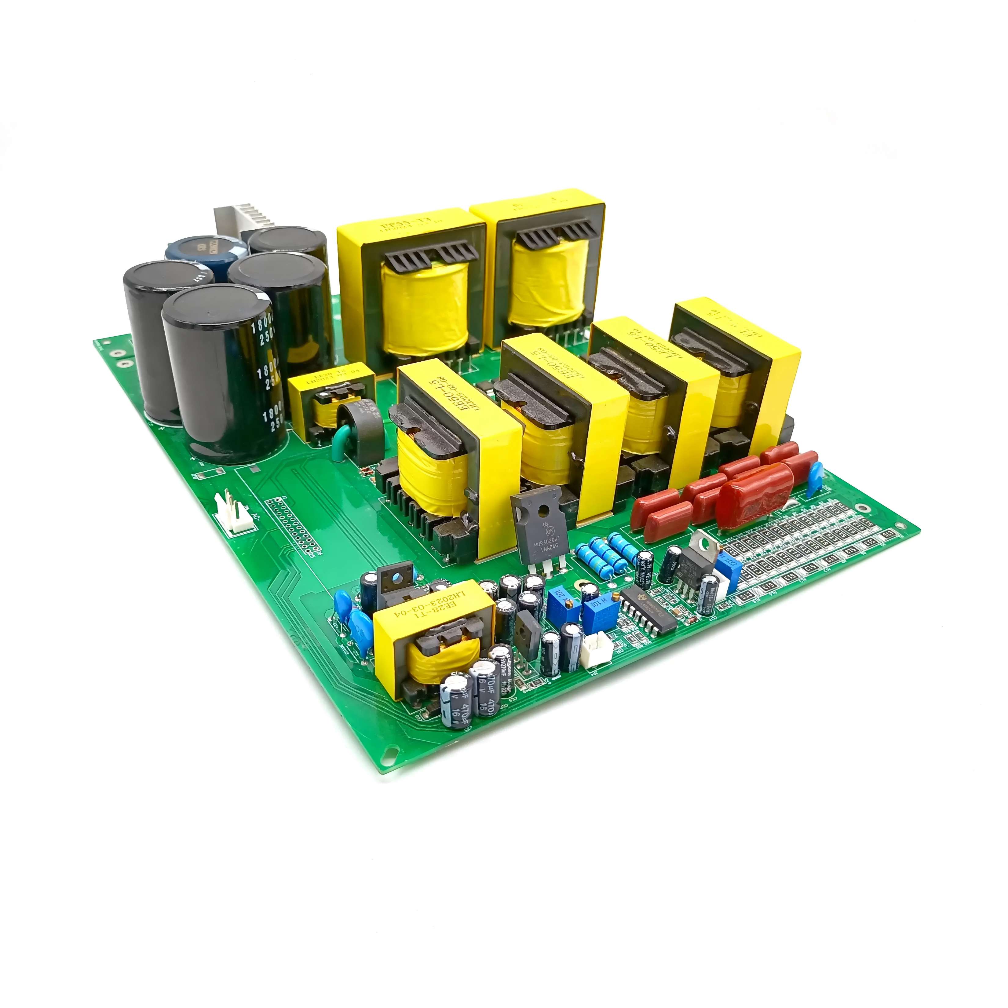
Multi-Layer PCB Evolution
Layer Stacking Techniques
Multi-layer boards are in many new devices today. These boards use stacking to fit more circuits in less space. Each layer does something different. Some layers move signals. Other layers give power or act as ground. How you stack the layers changes how well the device works.
Here is a table that lists important stacking factors and goals:
Factor/Objective
Description
Total Layers
The number of layers (like 4, 6, 8, or more) in the board.
Power/Ground Planes
Layers that supply power or act as ground for the circuit.
Layer Sequence
The order in which you arrange the layers.
Layer Spacing
The distance between layers, which changes how signals move.
Signal Layer Proximity
Signal layers should sit next to a power or ground plane.
Coupling of Layers
Signal layers need to be close to their planes for better performance.
Ground Planes
Power and ground planes should be close together to lower noise.
High-Speed Routing
High-speed signals travel on buried layers to reduce interference.
Multiple Ground Planes
More ground planes help lower impedance and cut down on unwanted signals.
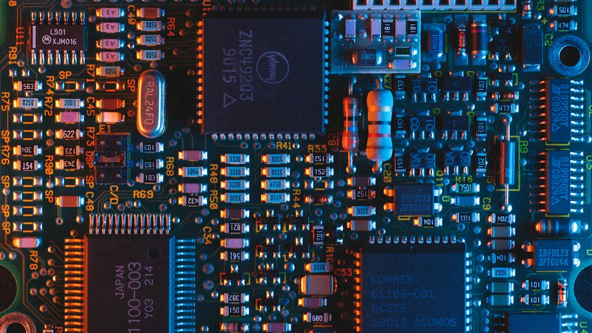
You can see that Printed Circuit Board designs now use more layers. AI server motherboards can have 18-22 layers. Some boards even have up to 30 layers. For example, a 24-layer board might have 12 signal layers, 8 power layers, and 4 ground layers. Stacking layers this way helps devices work faster and stay strong.
Addressing Complex Circuits
Multi-layer boards help with hard electronics problems. You can put more parts in a small space. This lets your phone or computer do more without getting bigger. Each layer has a job. Some layers carry signals. Others help with power or ground. If you plan the stack-up well, signals are better and there is less heat.
Here are some main benefits of multi-layer boards:
Advantage
Description
Increased component density
You can add more parts in the same space.
Improved signal integrity
Shorter paths and less noise make signals clearer and faster.
Enhanced design flexibility
You can create new and complex layouts for advanced devices.
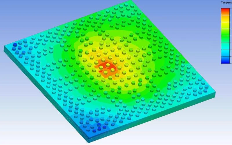
You also get better results because the stack-up lowers crosstalk and electromagnetic interference. Good design moves heat away from hot spots, so your device lasts longer.
Signal Integrity: Good layer order keeps signals clear and correct.
Thermal Management: Smart stack-up helps your device stay cool.
Manufacturing Challenges
Making multi-layer boards is hard. There are many problems to solve. You must line up each layer just right. If you do not, signals can fail or the board can break. Different materials grow at different speeds when hot, which can bend or crack the board.
Here are some common problems you might face:
Managing Thermal Expansion: Materials grow differently, which can cause trouble.
Interlayer Connectivity: You must line up layers to stop signal loss.
Signal Integrity: You need to control impedance and stop cross-talk.
Complex Assembly Processes: Stacking and bonding layers takes time and skill.
Higher Material Costs: More layers use more materials.
Increased Labor Costs: Skilled workers and longer work times cost more.
Advanced Equipment Requirements: Special machines are needed for careful work.
Increased Waste: More layers mean more leftover material.
Chemical Usage: You use many chemicals, which need safe handling.
Energy Consumption: Making these boards uses a lot of energy.
You also need to check for hidden problems like tiny cracks or signal trouble. Modern factories use special tests to find these before shipping. Here is a table that shows common failure types and how to fix them:
Failure Mode
Mitigation Strategy
Hidden defects (micro-cracks)
Use in-circuit testing and automated X-ray inspection to find problems.
Signal integrity issues
Design with ground planes next to signal layers and use controlled impedance.
Thermal management issues
Add thermal vias and use metal-core substrates for better heat control.
Multi-layer Printed Circuit Board technology lets you make strong and powerful devices, but you must design and build them carefully to avoid problems.
Advanced PCB Technologies
High-Density Interconnect (HDI)
HDI technology is in many new electronics. HDI boards use tiny traces and spaces. They also use microvias and thin materials. This design lets you fit more circuits in less space. You can add more parts without making the board bigger. HDI helps make smartphones and tablets powerful and small. Medical devices also use HDI for strong performance in small sizes. HDI gives better signal quality and faster speeds. You use less material, so devices are lighter.
Flexible and Rigid-Flex PCBs
Flexible and rigid-flex PCBs change how electronics are made. You can bend or fold these boards to fit small spaces. This is good for wearables, cameras, and medical tools. These boards are strong like rigid boards but can also bend. Here is a table that shows how these boards help:
Advantage
Description
Space Efficiency
Combines rigid and flexible regions for compact designs that fit into tight geometries.
Reliability
Reduces potential failure points by eliminating many connectors and interconnects.
Durability
Offers increased long-term reliability due to fewer interconnect points.
Reduced Assembly Costs
Simplifies installation by minimizing connections, reducing human error during assembly.
Rigid-flex PCBs are light and strong for new technology.
Fewer connections mean better signal quality.
Special shielding can help lower emissions.
Impact on Device Miniaturization
Advanced Printed Circuit Board technologies help make smaller devices. You can use Ball Grid Arrays (BGAs) for more connections in small spaces. BGAs help build powerful systems that fit in your hand. Wafer Level Chip Scale Packages (WLCSPs) give tiny chips with strong connections. These designs let you add more power and features to every device.
BGAs give more ways to connect chips and boards for speed and power.
WLCSPs let you use very small chips with tiny connections.
Devices can be lighter, faster, and more reliable.
With these new technologies, you can make electronics that are smaller, lighter, and stronger than ever before.
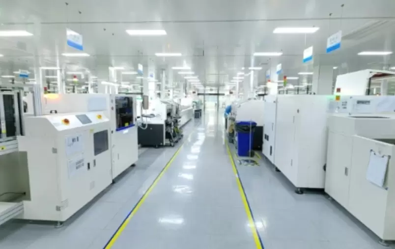
Printed Circuit Board Manufacturing Today
Quality Assurance and Testing
You want every Printed Circuit Board to work well. Factories use many tests to check for problems. These tests help find mistakes early. This means you can trust the boards you get. Here is a table with common testing methods:
Testing Method
Description
Automated Optical Inspection (AOI)
Uses cameras to look for surface problems and spots errors fast.
X-ray Inspection
Shows inside connections and finds hidden problems in thick boards.
In-Circuit Testing (ICT)
Checks how electricity moves and finds open or short circuits.
Functional Testing
Pretends the board is working in real life to see if it does its job.
Environmental Stress Testing
Puts boards in tough places to see if they last and work well.
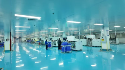
Benlida cares a lot about quality. The company uses ISO 9001 and IATF16949 systems. You get good order management with ERP and MaS. Benlida has AOI, X-ray, ICT testers, and BGA rework stations. These tools help fix problems before you get your boards.
Tip: Pick a company that tests well so your boards work every time.
Materials and Production Scale
You need good materials for strong boards. Factories use different materials for different jobs. Here is a table with common materials:
Material Type
Characteristics
FR4
Used a lot and works for most boards
Polyimide
Handles heat well and works for tough jobs
Ceramic
Lasts long and works for high-frequency boards
Metal Core PCBs
Moves heat away and bends easily
Benlida gives you many choices. You can pick FR-4, aluminum, ceramic, and more. The company makes boards with 1 to 48 layers. There are eight SMT lines for fast work. They can make over 50 million points each day. The factory is big, so you can order small or large batches. You get your boards quickly, sometimes in just five days.
You can order a few boards or many.
You get good boards every time, no matter how many you order.
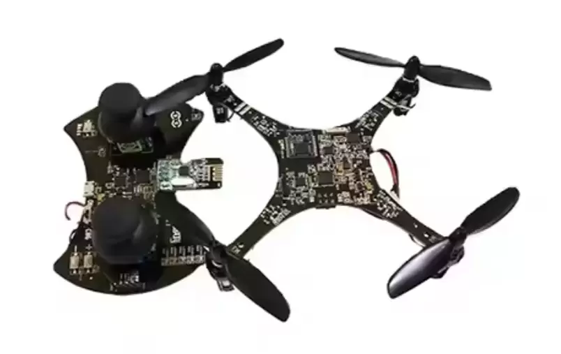
Industry Applications
Printed Circuit Boards are used everywhere today. They are in phones, computers, cars, and medical tools. Benlida helps over 380 customers around the world. Their boards are in electronics, cars, factories, and LED lights.
Benlida has lots of experience. The company has made boards for 18 years. You can trust them for easy or hard projects. Their testing and quality checks mean your boards last a long time.
Note: If you choose Benlida, you get new technology and help for your projects.
Future Trends in PCB Design
Emerging Materials and Processes
You will see big changes in PCB materials and how they are made. Scientists are finding new materials to make boards stronger and last longer. Some boards now use ceramics or special plastics. These can handle more heat and work at higher speeds. Factories are trying new ways to make boards. For example, they use lasers to make tiny paths for electricity. These changes help devices work faster and be more reliable.
Integration with New Technologies
PCBs are getting smarter and more connected every year. Here are some ways new technology is changing PCBs: - AI tools help engineers find the best way to lay out power and signals. This is important for devices that use the Internet of Things (IoT). - 5G networks are growing, so boards must handle higher frequencies. This means new designs for wireless PCBs and antennas. - More devices talk to each other, so boards must move lots of data quickly and safely. These changes let you use electronics in more places, like cars, hospitals, and smart homes.
Sustainability Considerations
You will face new problems when making PCBs safer for the planet. Some big problems are: - It is hard to take apart boards for recycling. - You must follow new rules about chemicals and waste. - You need to find materials that are better for the earth. To fix these problems, companies are:
1. Using materials that can be recycled.
2. Following rules like RoHS and REACH to keep bad chemicals out.
3. Stopping the use of PFAS, which can hurt people and nature.
Tip: Picking eco-friendly boards helps the earth and follows new laws.
You have seen how the Printed Circuit Board changed electronics over time.
Early inventions set the stage for new devices.
World War II pushed fast progress.
The space race and new parts made boards better.
Today, boards power almost every device you use.
Industry/Application
Growth and Reach
Automotive
Market grows to $13.39 billion by 2030
IoT
93 million US homes use smart devices by 2027
New ideas keep coming. Companies like Benlida lead the way, helping you use smarter and smaller technology every day.
FAQ
What is a multi-layer PCB?
A multi-layer PCB has three or more layers. These layers are stacked on top of each other. This gives more room for circuits. Devices like smartphones and computers use them. They help devices run faster and do more things.
Why do manufacturers use plated through-holes?
Plated through-holes are in double-layer and multi-layer PCBs. These holes link the layers together. This makes electrical connections stronger. Devices can work faster and last longer. They also help move heat away from hot parts.
How do flexible PCBs help modern devices?
Flexible PCBs are used in wearables, cameras, and medical tools. These boards can bend and fold easily. They fit into tight spaces inside devices. Flexible PCBs make things lighter and more dependable. Fewer connectors mean fewer problems.
What testing methods ensure PCB quality?
Factories use AOI, X-ray, and functional testing. These tests help find problems early. This means the boards are more reliable. AOI checks the surface for mistakes. X-ray looks inside the board for hidden issues. Functional testing checks if the board works right.
This website uses cookies to provide you with a safer and more personal experience. By accepting, you agree to the Cookie Policy and the use of cookies for advertising and analytics purposes.
 en
en


.jpg)
 WhatsApp