Electronic products continue to become more compact while delivering greater computing power, faster communication speeds, and expanded functionality. Smartphones now integrate advanced processors, multiple cameras, wireless communication modules, artificial intelligence capabilities, and high-capacity memory within devices small enough to fit comfortably in a pocket. Similar trends can be seen across automotive electronics, medical equipment, industrial automation systems, telecommunications infrastructure, and consumer electronics.
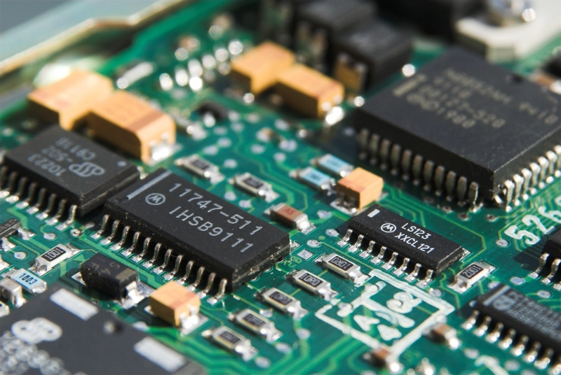
This increasing demand for performance creates significant challenges for PCB designers. More components must be integrated into smaller spaces while maintaining electrical performance, thermal stability, signal integrity, and manufacturing reliability. Traditional multilayer PCB structures can eventually reach physical limitations when routing density continues to increase.
HDI PCB technology has become one of the most important solutions to these challenges. By utilizing advanced interconnection structures such as microvias, blind vias, buried vias, and via-in-pad designs, engineers can significantly increase routing density without increasing board size.
The result is a new generation of electronic products that are smaller, lighter, faster, and more reliable than previous designs.
For industries ranging from automotive electronics to medical devices, High Density Interconnect PCB technology has become a key foundation for modern product development.
What Is an HDI PCB?
HDI PCB stands for High Density Interconnect Printed Circuit Board.
It refers to a circuit board designed with advanced interconnect technologies that allow significantly higher routing density compared with conventional multilayer PCBs.
Instead of relying on larger board dimensions or excessive layer counts, HDI PCB technology maximizes available routing space through optimized via structures and fine-feature manufacturing techniques.
Typical HDI PCB characteristics include:
- Laser-drilled microvias
- Blind vias
- Buried vias
- Via in Pad PCB technology
- Fine trace widths and spacing
- Sequential lamination structures
- High-density component placement
These features make it possible to support increasingly complex electronic systems while maintaining compact product dimensions.
A conventional multilayer PCB may use large mechanically drilled through-holes that occupy routing space across all layers. HDI structures reduce this limitation by creating more efficient interconnections that consume less board area.
This enables engineers to route thousands of signals within highly compact electronic assemblies.
Common HDI PCB Structures
HDI designs can be manufactured using several stack-up configurations depending on complexity requirements.
| Structure | Typical Application |
|---|
| 1+N+1 HDI PCB | Consumer Electronics |
| 2+N+2 HDI PCB | Networking Equipment |
| 3+N+3 HDI PCB | High-End Computing Systems |
| 8 Layer HDI PCB | Automotive and Industrial Electronics |
As device complexity increases, more sequential build-up layers can be added to provide additional routing capacity.
Why Traditional PCB Designs Face Limitations
Traditional PCB technology remains suitable for many industrial products. However, several design challenges continue to push manufacturers toward HDI solutions.
Increasing Component Density
Modern integrated circuits feature higher pin counts than ever before.
Processors, memory devices, communication modules, and FPGA components often use:
- Fine-pitch BGA packages
- High-speed interfaces
- Dense signal routing
- Compact footprints
Routing these connections through conventional through-hole vias quickly becomes inefficient.
Higher Data Transmission Speeds
Signal speeds continue to increase across multiple industries.
Applications such as:
- 5G communication
- Automotive radar
- AI computing
- High-speed networking
- Industrial automation
require PCB designs capable of maintaining signal integrity at extremely high frequencies.
Poor routing structures may introduce:
- Signal loss
- Crosstalk
- Reflection
- Electromagnetic interference
HDI technology helps minimize these challenges through shorter signal paths and optimized interconnections.
Miniaturization Requirements
Product manufacturers continuously seek smaller and lighter products.
Whether designing a wearable medical monitor, an industrial sensor, or an electric vehicle control module, engineers must maximize functionality within increasingly limited physical space.
HDI PCB technology directly supports this objective.
Key Technologies Behind HDI PCB Design
Several manufacturing technologies form the foundation of modern HDI PCB fabrication.
Microvia PCB Technology
Microvias are one of the most recognizable features of HDI boards.
Unlike conventional drilled vias, microvias are created using laser drilling processes and typically connect only adjacent layers.
The smaller size provides several advantages:
- Higher routing density
- Smaller pad requirements
- Improved signal performance
- More efficient use of PCB space
Microvia PCB technology is particularly valuable for BGA fan-out applications where routing space is limited.
Blind Via PCB Technology
Blind vias connect an outer layer to one or more internal layers without passing through the entire PCB.
This creates additional routing space that would otherwise be occupied by traditional through-hole vias.
Benefits include:
- Increased layer utilization
- Reduced routing congestion
- Better design flexibility
- Improved signal routing efficiency
Blind Via PCB structures are widely used in smartphones, networking equipment, and automotive control units.
Buried Via PCB Technology
Buried vias are located entirely within internal PCB layers.
Since they never reach the board surface, they free additional routing space for component placement and signal routing.
Buried vias contribute to:
- Higher interconnect density
- More compact layouts
- Better layer optimization
- Increased design flexibility
Via in Pad PCB Technology
Via in Pad PCB designs place vias directly within component mounting pads.
This approach is commonly used for:
- Fine-pitch BGA packages
- High-speed processors
- Dense memory arrays
Benefits include:
- Shorter electrical paths
- Improved thermal performance
- Better signal integrity
- Higher component density
Although manufacturing complexity increases, Via in Pad PCB technology has become essential for many advanced electronic products.
How HDI PCB Supports Smaller Electronic Devices
Miniaturization remains one of the primary reasons manufacturers adopt HDI PCB technology.
Every square millimeter inside an electronic product has value.
By reducing via size and increasing routing density, HDI technology enables engineers to place more circuitry within the same board area.
This allows designers to:
- Reduce PCB dimensions
- Decrease product weight
- Increase functionality
- Improve packaging efficiency
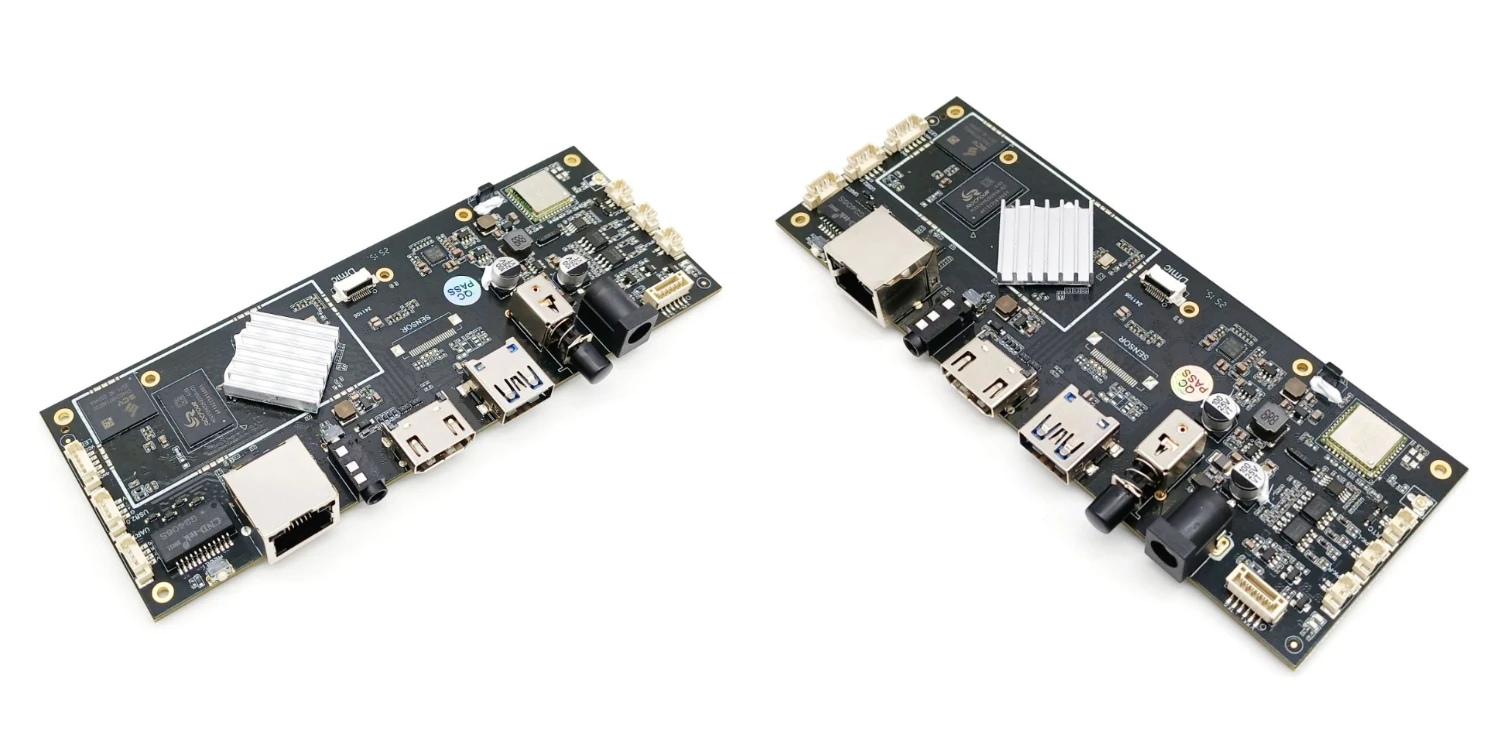
A smartphone that previously required two circuit boards may now integrate the same functionality onto a single HDI board.
Similarly, automotive control modules can incorporate more processing power without increasing enclosure size.
Medical devices also benefit significantly.
Portable monitoring equipment, wearable health devices, and handheld diagnostic tools all depend on compact electronic architectures made possible by HDI PCB technology.
How HDI PCB Improves Performance and Reliability
The advantages of HDI PCB technology extend far beyond miniaturization.
Electrical performance improvements often become equally important.
Shorter Signal Paths
Smaller interconnect structures reduce overall routing length.
Shorter electrical paths contribute to:
- Faster signal transmission
- Reduced latency
- Lower insertion loss
- Improved timing control
These benefits become increasingly important in high-speed digital applications.
Better Signal Integrity
Signal integrity challenges grow as transmission frequencies increase.
HDI structures help minimize:
- Crosstalk
- Reflection
- Noise coupling
- Electromagnetic interference
This supports reliable operation in demanding environments.
Enhanced Thermal Management
Higher component density often generates additional heat.
Advanced HDI structures can improve thermal transfer paths, particularly when combined with via-in-pad technology.
Improved thermal performance helps maintain long-term reliability.
Increased Mechanical Reliability
Smaller interconnect structures may appear fragile, but properly manufactured HDI boards often demonstrate excellent reliability.
Carefully controlled fabrication processes produce:
- Strong copper adhesion
- Reliable via connections
- Consistent layer bonding
- Improved fatigue resistance
These characteristics are particularly valuable in automotive and industrial applications where vibration and temperature cycling occur regularly.
Applications of HDI PCB Across Industries
HDI technology supports a wide range of modern industries.
Automotive PCB Applications
Vehicle electronics continue to increase rapidly.
Modern vehicles contain dozens of electronic control units responsible for:
- Engine management
- Battery control
- Advanced driver assistance systems
- Radar modules
- Infotainment systems
Automotive PCB designs increasingly rely on HDI structures to meet space and performance requirements.
Medical Device PCB Applications
Medical equipment manufacturers require compact, reliable, and highly accurate electronic systems.
Common examples include:
- Portable diagnostic equipment
- Patient monitoring devices
- Surgical instruments
- Imaging systems
- Wearable healthcare products
HDI technology enables smaller devices without sacrificing performance.
Industrial PCB Applications
Industrial automation systems often operate in demanding environments.
Applications include:
- PLC controllers
- Industrial sensors
- Robotics
- Motor drives
- Factory automation equipment
HDI PCB technology supports higher functionality while maintaining reliability.
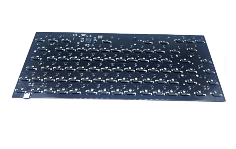
Consumer Electronics
Consumer products represent one of the largest HDI markets.
Examples include:
- Smartphones
- Tablets
- Smartwatches
- Laptops
- Gaming devices
Nearly every premium consumer electronic device relies on HDI PCB structures.
How to Choose a Reliable HDI PCB Manufacturer
Selecting the right HDI PCB Manufacturer plays a major role in project success.
HDI production requires specialized equipment, process control, and engineering expertise.
Several factors should be evaluated during supplier selection.
Manufacturing Capability
Not every PCB factory can produce advanced HDI structures.
Evaluate capabilities such as:
- Laser drilling
- Sequential lamination
- Fine-line processing
- Via filling
- Controlled impedance manufacturing
Quality Control Systems
Consistent quality is essential.
Review:
- Process certifications
- Inspection procedures
- Reliability testing
- Yield performance
Engineering Support
Complex HDI designs often require collaboration between designers and fabricators.
Strong engineering support can help optimize manufacturability while reducing production risks.
Industry Experience
Experience with Automotive PCB, Medical Device PCB, and Industrial PCB projects often indicates stronger process maturity and reliability.
Future Trends in HDI PCB Development
HDI PCB technology continues to evolve alongside the electronics industry.
Several trends are shaping future development.
Higher Layer Counts
Products requiring advanced computing power will continue adopting increasingly complex HDI structures.
8 Layer HDI PCB and 3+N+3 HDI PCB configurations are becoming more common in high-performance applications.
Ultra-Fine Interconnect Technology
Future products will require:
- Smaller microvias
- Narrower traces
- Higher component density
Manufacturing capabilities will continue advancing to meet these demands.
Automotive Electrification
Electric vehicles are significantly increasing demand for sophisticated electronic control systems.
HDI PCB adoption is expected to grow throughout the EV supply chain.
Medical Device Innovation
Portable healthcare equipment and remote monitoring systems continue driving demand for compact, highly reliable PCB technologies.
AI and High-Speed Computing
Artificial intelligence hardware requires enormous processing power and data throughput.
HDI technology will remain essential for supporting next-generation computing architectures.
HDI PCB technology has become one of the most important foundations of modern electronics manufacturing. Through advanced interconnect structures such as Microvia PCB, Blind Via PCB, Buried Via PCB, and Via in Pad PCB designs, engineers can achieve dramatically higher routing density while maintaining excellent electrical performance and reliability.
From smartphones and medical devices to automotive control systems and industrial automation equipment, HDI solutions help manufacturers deliver products that are smaller, faster, and more capable than ever before.
As electronic systems continue to increase in complexity, demand for advanced High Density Interconnect PCB solutions will continue to expand. Companies seeking long-term competitiveness in modern electronics manufacturing increasingly view HDI technology not simply as an option, but as a critical design and production capability that supports future innovation.
About the author:

Sonic Yang
As a major in Electronics and Mechanical Automation, Sonic has been engaged in PCB design, R&D, and manufacturing of electronics for around 22 years, as the engineering director, and coordinates with the supply chain(components and CNC parts), providing professional support and consulting for global customers.
 en
en


 WhatsApp