Home > Blog > Industry News > Understanding, Applications, and Advancements in Printed Circuit Board Technology
Understanding, Applications, and Advancements in Printed Circuit Board Technology
Share
Nov 27
Source:
You rely on printed circuit boards every day, whether you use a smartphone, a medical device, or a car. Printed Circuit Board Technology forms the backbone of modern electronics by connecting and supporting electronic components. Companies like Benlida have pushed innovation in this field, using advanced manufacturing to deliver reliable, high-quality PCBs for a wide range of applications. You benefit from these advancements each time you interact with electronic devices.
Key Takeaways
Printed circuit boards (PCBs) are essential for connecting and supporting electronic components in devices like smartphones and medical equipment.
PCBs come in various types, including single-sided, double-sided, and multi-layer, each designed for specific applications and complexity.
Modern advancements in PCB technology, such as miniaturization and high-density interconnects, allow for smaller, faster, and more reliable electronics.
Manufacturers use eco-friendly materials to create PCBs, reducing environmental impact and meeting new regulations.
Quality assurance methods, like automated optical inspection, ensure that every PCB functions correctly and meets high standards.
Flexible and rigid-flex PCBs are ideal for devices that need to bend or fit into tight spaces, making them popular in wearables and medical devices.
Emerging technologies, such as AI in design and smart manufacturing, are shaping the future of PCB production and efficiency.
Staying informed about PCB trends helps you choose the right technology for your projects and ensures reliable performance in your devices.
PCB Technology Overview
What Is a PCB?
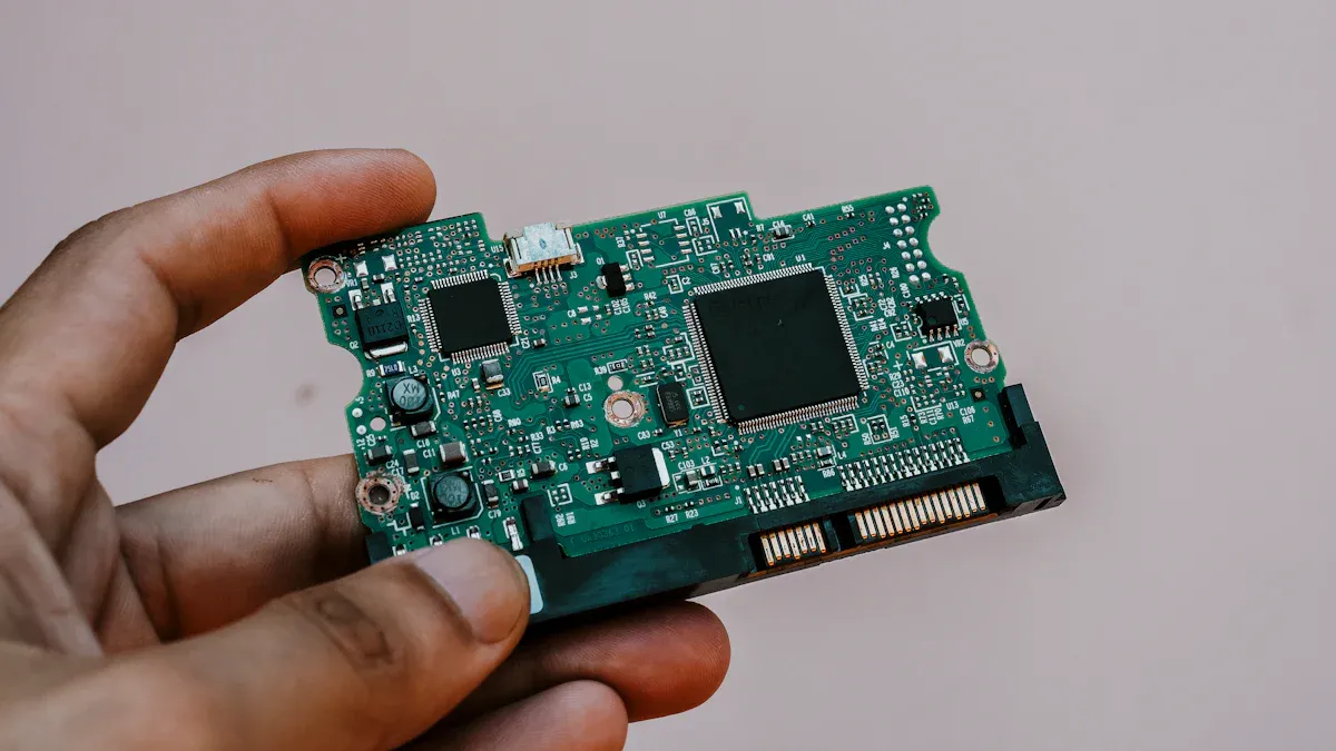
You see printed circuit boards, or PCBs, inside almost every electronic device you use. A PCB is a flat board that holds and connects electronic components. Manufacturers use materials like fiberglass or plastic for the base. They add thin layers of copper to create pathways for electricity. These copper traces guide electrical signals between different parts of a device. Printed Circuit Board Technology allows you to enjoy smaller, faster, and more reliable electronics.
Key Functions
A PCB does much more than just hold parts in place. It acts as the foundation for electronic circuits. Here are the main functions you will find in every PCB:
Connects electrical components to one another in an electronic circuit.
Provides a structure for mounting components through soldering.
Enables electrical interconnections between layers using vias.
You can think of a PCB as the roadmap for electricity inside your devices. Each trace and connection ensures that signals travel to the right place at the right time.
Tip: When you look at a PCB, you see a network of lines and dots. These are the copper traces and pads that make everything work together.
Importance in Electronics
Printed Circuit Board Technology plays a vital role in modern electronics. You depend on PCBs for everything from simple gadgets to advanced machines. PCBs come in several types, each designed for specific needs:
Single-sided PCBs have one layer of conductive material. You find them in basic electronics like remote controls.
Double-sided PCBs allow components on both sides. These boards support more complex designs, such as power supplies.
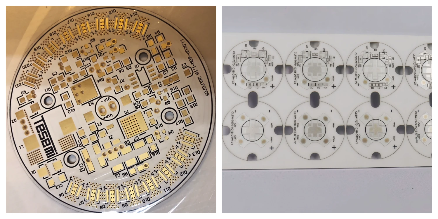
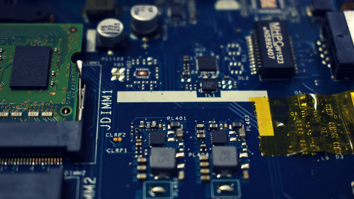
Multilayer PCBs contain several layers of copper traces. You see these in high-tech applications like servers and medical devices.
As technology advances, PCBs have evolved to support faster and more complex systems. You benefit from this progress every time you use a smartphone, a computer, or even a medical monitor. Printed Circuit Board Technology continues to drive innovation, making electronics more powerful and efficient.
History and Evolution
Early Innovations
Before you had printed circuit boards, engineers used a method called point-to-point wiring. This approach involved connecting each component with individual wires. While it worked for early devices, it caused many problems. You can see the main features of point-to-point wiring in the table below:
Key Features of Point-to-Point Wiring
Description
Bulky and inefficient wiring
This led to reliability issues.
Time-consuming assembly
This made production slow and expensive.
Prone to failures
Wires could loosen and short-circuit over time.
Used in early devices
Examples include radios, telephones, and electrical equipment.
This method made devices bulky and difficult to repair. As electronics became more complex, you needed a better solution.
Major Milestones
You can trace the progress of Printed Circuit Board Technology through several important milestones:
1920s-1930s: Early PCBs used wire-wrap technology, which was slow and hard to manage.
1940s: Paul Eisler invented the modern PCB, using a flat board with conductive pathways. The military first used this technology.
1950s: PCBs entered consumer electronics, making products more reliable and durable.
1960s: Multilayer PCBs appeared, allowing for more complex and compact designs.
1980s: Surface-Mount Technology (SMT) changed how you assemble PCBs, making them smaller and more efficient.
1990s: New techniques like laser drilling and High-Density Interconnect (HDI) technology improved performance.
2000s: Flexible and rigid-flex PCBs became popular for new applications.
Modern Innovations: High-frequency PCBs and printed electronics now support advanced devices.
Each step made electronics smaller, faster, and more reliable.
Modern Developments
Today, you benefit from advanced manufacturing techniques that have transformed PCB design. Direct Imaging lets you create finer lines and better layer alignment. Additive manufacturing reduces waste and gives you more freedom in design. These innovations help you get prototypes faster and with fewer defects. As a result, modern PCBs support the compact and powerful devices you use every day. Printed Circuit Board Technology continues to evolve, making electronics more efficient and dependable for the future.
PCB Structure and Materials
Understanding the structure and materials of a printed circuit board helps you see how these essential components power your devices. Each layer and material plays a specific role in making sure your electronics work safely and efficiently.
Layers and Composition
A PCB contains several layers, each with a unique function. You can see the standard layers in a multi-layer board and their roles in the table below:
Layer Type
Function
Inner Layers
Provide low-impedance power distribution, stabilize voltage levels, and minimize noise.
Copper Layers
Facilitate signal transmission, power distribution, and heat dissipation.
Solder Mask
Protects copper traces from oxidation, reduces solder bridge risks, and provides electrical insulation.
Silkscreen
Offers labeling and identification for assembly, testing, and maintenance of the PCB.
Substrate Types
You find the substrate at the core of every PCB. This base layer gives the board its strength and shape. Most PCBs use materials like FR-4, which combines epoxy resin with woven fiberglass. Some boards use CEM-1, CEM-3, or FR-2 for cost savings or specific performance needs. The substrate must handle heat and provide a stable platform for the other layers.
Conductive Paths
Copper layers form the conductive paths on a PCB. These thin copper traces act like tiny roads, guiding electricity and signals between components. You rely on these paths for fast and accurate communication inside your devices. Good design ensures each area of the board can handle the right amount of current and voltage.
Protective Coatings
A solder mask covers the copper traces to protect them from oxidation and accidental solder bridges. This green (or sometimes other colored) layer also provides electrical insulation. The silkscreen layer sits on top, giving you labels and markings that help with assembly and repair.
Common Materials
Manufacturers choose materials based on the needs of your device. Here are some of the most common materials and their properties:
Material
Composition
Flame Retardant
Thermal Performance
Applications
FR-4
Epoxy resin + Woven fiberglass
Yes (UL 94 V-0)
High
High mechanical strength and thermal stability
CEM-3
Epoxy resin + Woven fiberglass
Yes (UL 94 V-0)
High (slightly lower than FR-4)
Cost-effective for double-sided boards
CEM-1
Epoxy resin + Woven fiberglass
Yes
Moderate
Used for cost reduction
FR-2
Epoxy resin + Woven fiberglass
Yes
Moderate
Low-cost, not for high heat or moisture
You also see thermoset materials like epoxy, polyimide, and aramid, which have high melting points and cannot be remelted. Thermoplastic materials, such as PTFE, can be reshaped and have lower melting points. Most PCB materials combine copper, resin, and glass. The resin type affects properties like heat resistance and electrical performance.
How PCBs Work
A PCB works by guiding electricity and signals through copper traces. You can think of these traces as highways for electrical current. Components such as resistors, capacitors, and chips connect to these paths. Signals travel along the traces, carrying information between parts of your device. Careful design allows each section of the board to handle different currents and voltages, which protects your electronics from damage.
Printed Circuit Board Technology brings all these elements together, allowing you to enjoy reliable and efficient electronic devices every day.
Manufacturing and Assembly
Design Process
You start every successful PCB project with a careful design process. This step shapes how your board will function and how reliable it will be. Here is a typical sequence you follow when designing a printed circuit board:
Understand the electrical parameters for your project.
Create the schematic diagram that shows how each component connects.
Use a schematic capture tool to lay out your PCB.
Design your PCB stackup, which defines the arrangement of layers.
Set design rules and requirements for spacing, trace width, and clearances.
Place your components in the best positions for performance and manufacturability.
Insert drill holes for mounting and electrical connections.
Route the traces that connect your components.
Add labels and identifiers for assembly and troubleshooting.
Generate design and layout files, such as Gerber files, for manufacturing.
Tip: Using advanced design software helps you avoid errors and speeds up the process.
Benlida’s engineering team uses these steps to create everything from simple single-layer boards to complex multi-layer, HDI, ceramic, LED/aluminum, FPC, and rigid-flex PCBs. You benefit from their experience and attention to detail at every stage.
Fabrication Steps
Once you finish your design, you move to fabrication. This process transforms your digital design into a physical board. Each stage uses specialized technology to ensure accuracy and quality.
Stage
Description
Imaging
The layout is imaged onto copper-clad laminates.
Etching
Excess copper is removed to reveal traces and pads.
Layer Stackup
Board materials are laminated at high temperatures to create the stackup.
Drilling
Holes are drilled for mounting, pins, and vias.
Surface Etching
Surface layers are etched to define traces and pads.
Plating
Pin holes and via holes receive a conductive coating.
Protective Coating
A solder mask is applied to protect the copper.
Silkscreen Printing
Markings, logos, and indicators are printed on the surface.
Finishing
An optional finish is added to exposed copper areas.
Etching
You remove unwanted copper from the board during etching. This step reveals the precise pathways that carry signals and power. Careful control ensures that traces remain sharp and accurate.
Drilling
You drill holes for mounting components and creating electrical connections between layers. High-speed machines make these holes with great precision. This step is essential for multi-layer and HDI boards.
Plating
You add a thin layer of metal to the drilled holes during plating. This process creates reliable electrical connections between layers. Plating also strengthens the holes, making your board more durable.
Assembly Techniques
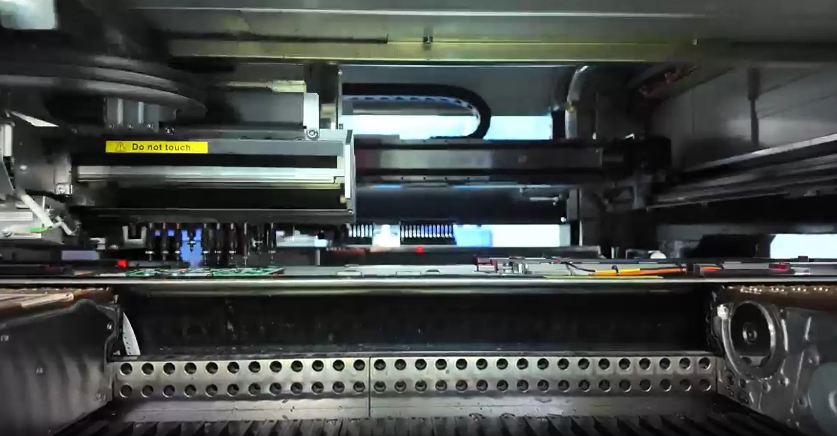
After fabrication, you assemble the board by placing and soldering components. You can use surface-mount technology (SMT) for small, high-density parts or through-hole assembly for larger components. Benlida uses advanced assembly lines and automated equipment to ensure accuracy and speed. You benefit from their quick lead times and strict quality controls, which include automated optical inspection (AOI), flying probe testing, and functional testing. These methods help deliver reliable PCBs for every application.
Quality Assurance
You want every printed circuit board in your device to work perfectly. Quality assurance makes this possible. At each stage of manufacturing and assembly, you see strict checks that help catch problems early. This process keeps your electronics safe and reliable.
Benlida uses advanced quality assurance methods to deliver dependable PCBs. You benefit from their expertise in multi-layer, HDI, ceramic, LED/aluminum, FPC, and rigid-flex boards. Their team follows a detailed inspection process, so you get products that meet the highest standards.
You can find several key methods used to check the quality of PCBs:
Method
Description
Benefits
AOI (Automated Optical Inspection)
Uses high-resolution cameras and image processing to detect defects.
Fast identification of visual defects, especially in high-volume manufacturing.
In-Circuit Testing (ICT)
Tests electrical properties using a fixture to contact test points.
Efficient and reliable for verifying correct installation and functionality of components.
Flying Probe Testing
Uses probes to test specific points without powering the circuit.
Accurate and flexible, suitable for low- to medium-production volumes.
You see AOI used to spot issues like misaligned components or soldering mistakes. High-resolution cameras scan the board and compare it to the design. This method quickly finds visual defects, which helps prevent faulty boards from reaching you.
In-circuit testing (ICT) checks the electrical properties of each component. You use a fixture called a "bed of nails" to touch test points on the board. This test confirms that every part works as it should. ICT is very effective for large production runs.
Flying probe testing gives you flexibility. Instead of using a custom fixture, this method uses moving probes to touch different points on the board. You can test resistance, capacitance, and shorts without powering the circuit. This approach works well for prototypes and small to medium batches.
Note: Benlida combines these methods with functional testing to make sure every PCB performs as expected in real-world conditions.
You also benefit from Benlida’s quick lead times. Their efficient quality assurance process means you get your boards faster, without sacrificing reliability. Each PCB goes through multiple checks, from automated inspection to hands-on testing. This attention to detail helps you avoid costly failures and keeps your devices running smoothly.
When you choose a manufacturer with strong quality assurance, you gain peace of mind. You know your electronics will work as designed, whether you use them in consumer gadgets, medical devices, or advanced robotics.
Types of PCBs
Single-Sided
You often find single-sided printed circuit boards in basic electronic devices. These boards have copper traces on only one side. All components sit on the opposite side. This simple structure makes them easy to design and manufacture. You can see how single-sided PCBs compare to other types in the table below:
Feature
Single-Sided PCB
Other Types (Double-Sided, Multi-Layer)
Conductive Layers
One layer of copper traces
Two or more layers of copper traces
Component Placement
Components mounted on the opposite side
Components can be mounted on both sides
Complexity
Simpler design and manufacturing
More complex design and manufacturing
Cost
Generally lower cost
Higher cost due to complexity
Typical Applications
Consumer electronics, power supplies, industrial controls, educational projects
More complex devices requiring compact circuitry and more components
You use single-sided PCBs in products like calculators, radios, and simple power supplies. These boards offer a cost-effective solution for straightforward circuits. You benefit from their reliability and ease of repair.
Double-Sided
Double-sided PCBs take your designs a step further. These boards have copper traces on both sides. You can mount components on either side, which increases the number of parts you can use. This structure allows for more complex circuits in a compact space.
Advantages of double-sided PCBs include:
You can fit more components on the same board size.
These boards are essential for modern devices with limited space.
You achieve higher circuit density, which supports advanced features.
You often see double-sided PCBs in vending machines, dashboards, and industrial controls. They help you avoid point-to-point soldering, making assembly faster and more reliable.
However, you should know about some challenges:
The design becomes more complex.
Fabrication and assembly require more skill.
Testing and rework can be difficult.
You choose double-sided PCBs when you need more functionality without increasing the size of your device.
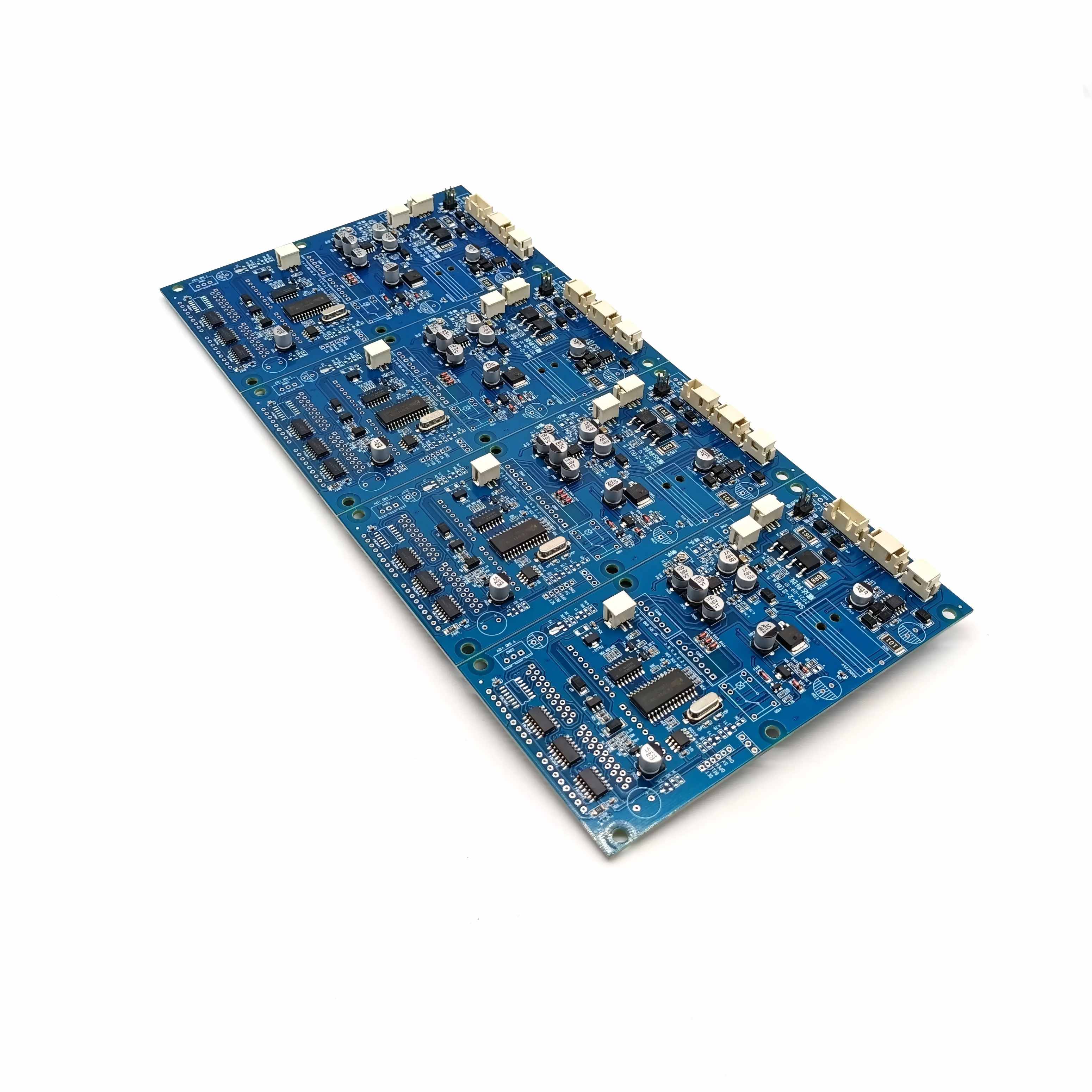
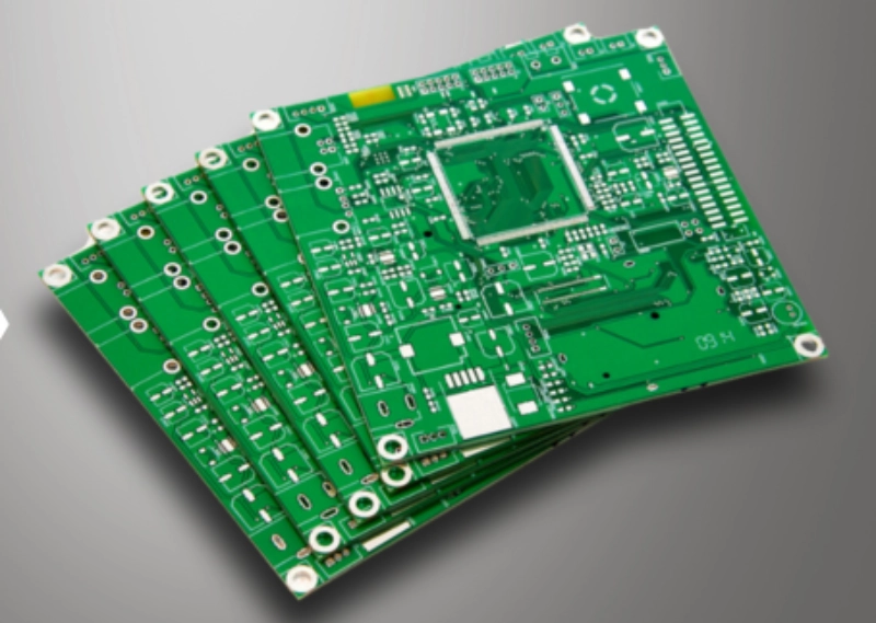
Multi-Layer
Multi-layer PCBs give you even greater possibilities. These boards stack three or more layers of copper traces, separated by insulating material. You use them in smartphones, computers, and medical equipment.
With multi-layer PCBs, you gain:
Enhanced design flexibility for intricate circuits.
Improved signal integrity, which reduces electromagnetic interference and crosstalk.
Higher component density without making the board larger.
Efficient power distribution across layers, which minimizes voltage drops and power loss.
You rely on multi-layer PCBs for devices that demand high performance and compact size. These boards support advanced features and help you create powerful, reliable electronics.
Tip: When you need to pack more technology into a small space, multi-layer PCBs are your best choice.
Flexible and Rigid-Flex
You often see flexible and rigid-flex printed circuit boards in devices that need to bend or fit into tight spaces. These boards combine the best of both worlds: the flexibility of a bendable circuit and the strength of a rigid board. You can use them in products that require movement, folding, or complex shapes.
Here is a table that shows the unique features and benefits of flexible and rigid-flex PCBs:
Feature/Benefit
Description
Hybrid Solution
Combines rigid and flexible technologies for new design possibilities.
Mechanical Stability
Can bend, fold, or twist without losing electrical performance.
High Shock Resistance
Withstands high-shock and high-vibration environments.
Increased Density
Allows for more compact designs while reducing weight.
Dynamic Flex Connections
Supports numerous bending cycles without failure.
Simplified Assembly
Reduces interconnections, enhancing reliability.
Cost Efficiency
Potentially lowers production costs in complex assemblies.
Industry Suitability
Ideal for aerospace, defense, medical technology, and avionic systems.
You benefit from these boards in products like medical devices, cameras, and wearable electronics. Flexible and rigid-flex PCBs help you create lighter, smaller, and more reliable devices. You also find them in aerospace and defense, where shock resistance and durability matter most.
Tip: If you need a circuit board that can move or fit into a unique shape, flexible and rigid-flex PCBs are your best choice.
High-Frequency
You use high-frequency printed circuit boards when your device needs to handle fast signals or high-speed data. These boards use special materials that keep signals clear and strong, even at high speeds. You often find high-frequency PCBs in advanced technology.
Here are some common applications for high-frequency PCBs:
Telecommunications, such as cell networks, satellites, and antennas
Automotive systems, including driver assistance, navigation, and electric vehicles
Medical devices, like MRIs, CT scanners, and patient monitors
Aerospace and defense, including radar, guidance systems, and drones
You rely on high-frequency PCBs for clear communication, accurate data, and fast response times. These boards help you build devices that work well in demanding environments.
Specialized Boards
You can choose from many types of specialized printed circuit boards to meet your project’s needs. Each type serves a unique purpose and fits specific industries.
Here are some examples of specialized PCBs and their uses:
Single-layer PCBs: You find these in simple devices like electronic toys, remote controls, and basic household gadgets.
Double-layer PCBs: You use these to route signals on both sides of the board, saving space and creating efficient current paths.
Multi-layer PCBs: You rely on these for advanced systems that need high performance.
Flexible PCBs (Flex PCBs): You use these in devices that need to bend or fit into tight spaces.
Rigid-Flex PCBs: You see these in medical, defense, and consumer electronics.
Specialized PCBs appear in many industries:
Consumer Electronics: Smartphones, laptops, tablets, and smart home appliances
Automotive Industry: Engine control units, advanced safety systems, and electric vehicles
Medical Industry: Medical imaging equipment, heart monitors, and surgical tools
Defense and Aerospace Industry: Encrypted communication equipment and navigation systems
Industrial Manufacturing and Automation: PLCs and smart sensors
Telecommunications and 5G: Cellular base stations and smart antennas
Smart Transportation and Railway Systems: Railway management and safety systems
Smart Agriculture: Environmental monitoring and smart irrigation systems
You can select the right specialized board to match your device’s requirements and industry standards. This choice helps you achieve the best performance and reliability for your application.
Applications Across Industries
Consumer Electronics
You interact with printed circuit boards every day through your favorite gadgets. PCBs power smartphones, tablets, laptops, and smart home devices. You rely on these boards for fast performance, compact size, and long battery life. Manufacturers use advanced PCB designs to fit more features into smaller spaces. You see this in wireless earbuds, fitness trackers, and gaming consoles. Benlida supplies high-quality PCBs for many consumer electronics, ensuring your devices stay reliable and efficient.
Tip: Next time you use your TV remote or charge your smartwatch, remember that a PCB makes it all possible.
Medical Devices
You trust medical devices to keep you healthy and safe. PCBs play a critical role in these tools. You find them in heart monitors, imaging equipment, and portable diagnostic devices. Medical PCBs must meet strict standards for safety and reliability. Manufacturers often use aluminum PCBs in these applications. Aluminum boards provide excellent thermal conductivity, which helps manage heat in temperature-sensitive environments. They also resist harsh conditions and can handle sterilization processes. This makes them ideal for use in hospitals and clinics.
Aluminum PCBs manage heat, keeping devices safe during long use.
These boards last longer because they resist damage from cleaning and sterilization.
You get consistent performance, even in demanding medical settings.
Benlida delivers durable and precise PCBs for medical technology, supporting your health and well-being.
Automotive Systems
You depend on PCBs every time you drive. Modern vehicles use printed circuit boards in almost every system. You see them in airbag controls, anti-lock brake systems, and anti-theft features. PCBs also power audio-video systems, climate control, and digital displays. They help manage engine timing, ignition, and power steering. Even windshield wipers and lamp controls rely on PCBs for smooth operation. Advanced cars use PCBs in transmission sensors and power converters, making your ride safer and more comfortable.
Airbag and safety controls
Engine and ignition management
Entertainment and navigation systems
Lighting and climate control
Transmission and sensor networks
Benlida’s automotive-grade PCBs meet high standards for durability and performance. You benefit from safer, smarter, and more reliable vehicles on the road.
Industrial Automation
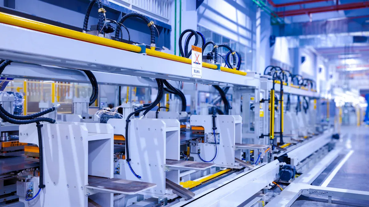
You see printed circuit boards at the heart of modern factories and production lines. PCBs control robots, sensors, and machines that help companies make products faster and with fewer errors. You rely on these boards for tasks like sorting, packaging, and quality checks. In industrial automation, PCBs must handle tough conditions. They face heat, dust, and constant vibration. Manufacturers use strong materials and protective coatings to keep these boards working day after day.
You find PCBs in programmable logic controllers (PLCs), motor drives, and smart sensors. These devices help you monitor and control every step of the manufacturing process. With advanced PCBs, you can collect data, spot problems early, and keep machines running smoothly. Benlida supplies reliable PCBs for industrial automation. Their boards support high-speed communication and precise control, which helps factories stay efficient and safe.
Tip: When you see a robot arm moving parts on an assembly line, a PCB is making every move possible.
Aerospace and Defense
You depend on printed circuit boards for safety and performance in airplanes, satellites, and defense systems. These boards must meet strict standards because failure is not an option. PCBs in aerospace and defense face extreme temperatures, strong vibrations, and high levels of stress. They must also be lightweight and compact to fit into tight spaces.
Here are some key requirements for aerospace and defense PCBs:
Standard
Description
IPC-6012
Sets rules for reliability and performance in rigid PCBs used in aerospace applications.
IPC-A-610
Provides guidelines for visual inspection to ensure quality standards are met.
MIL-PRF-31032
Covers material selection, fabrication, and testing for military PCBs.
ISO 9001
Ensures consistent quality in manufacturing processes.
You also need to consider these challenges:
PCBs must survive extreme temperatures and mechanical shocks.
Designs often include redundancy to keep systems running if one part fails.
High-frequency signals require careful layout to avoid interference.
Size and weight must stay low without losing performance.
Benlida delivers PCBs that meet these high standards. Their boards help keep aircraft, satellites, and defense equipment reliable and safe.
Emerging Technologies
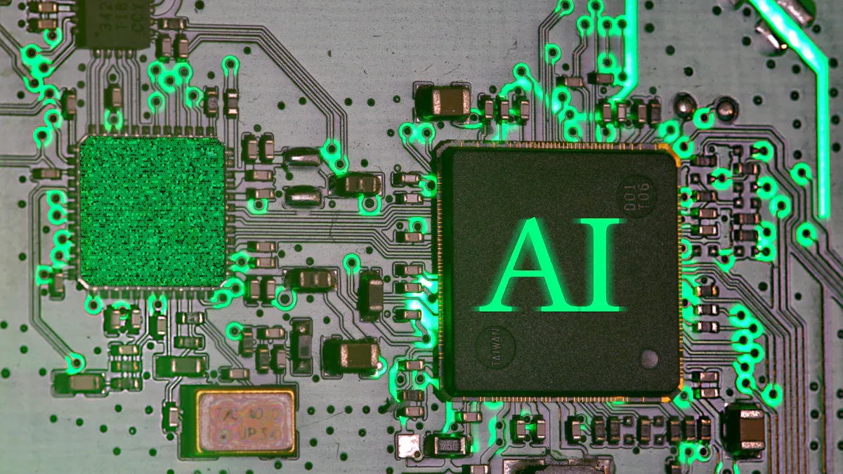
You see printed circuit boards powering the latest breakthroughs in technology. In fields like AI robotics and surveillance, PCBs must support fast data processing and smart decision-making. Automated assembly lines now use machine vision and advanced positioning methods to place components with high accuracy. Sometimes, poor lighting or blocked views can cause problems. New vision-free, model-agnostic methods let robots learn and adapt, making assembly more flexible and efficient. This is important for AI-driven devices that need to change quickly.
AI also changes how you design PCBs. Advanced algorithms help create complex layouts that use space better and work faster. AI tools can spot design flaws before you build the board, saving time and money. This is key for rapid development in AI robots and surveillance systems. Benlida supports these new technologies by providing high-quality PCBs for smart robots, security cameras, and other advanced devices. You benefit from faster, smarter, and more reliable electronics in your daily life.
Note: As technology moves forward, you will see PCBs become even more important in shaping the future of smart machines and connected systems.
Advancements in Printed Circuit Board Technology
Miniaturization
You see miniaturization shaping the future of electronics. As devices get smaller, you expect more features packed into less space. Printed Circuit Board Technology now supports higher density and greater functionality. This progress lets you carry powerful tools in your pocket or wear them on your wrist.
Here is a table that shows how miniaturization impacts device design:
Advancement Type
Impact on Device Design
Higher Density
Enables more functionality in a smaller space, improving signal integrity and reducing power consumption.
Increased Reliability
Minimizes damage risks from environmental factors, enhancing performance and durability.
Greater Functionality
Allows for more features and complex designs in compact PCBs, meeting diverse application needs.
Smaller Size
Facilitates portability and efficient space usage in devices, leading to user-friendly designs.
You notice these changes in many areas:
Wearable technology becomes lighter and more comfortable.
IoT devices fit into everyday objects, making your life smarter.
Computers and smartphones run faster while using less energy.
Miniaturization lets you enjoy advanced electronics that are easy to carry and use. You benefit from devices that last longer and perform better, even in tough environments.
High-Density Interconnects
High-density interconnect (HDI) technology changes how you design and use electronic devices. You can fit more connections into a smaller area, which means your devices become more compact and powerful. HDI boards use fine lines, small vias, and multiple layers to achieve this high wiring density.
With HDI technology, you gain several advantages:
You get more compact designs because wiring density increases.
Signal integrity improves due to shorter connections and lower power needs.
You can combine the functions of several boards into one HDI PCB, which boosts performance.
You see HDI boards in smartphones, tablets, and advanced medical equipment. These boards help you enjoy faster speeds, better reliability, and more features in your favorite devices.
Surface-Mount Technology
Surface-mount technology (SMT) changes the way you build and use electronics. Instead of inserting component leads through holes, you place components directly onto the surface of the PCB. This method saves space and allows for smaller, lighter devices.
SMT offers you several benefits:
You can fit more components on each board, which increases functionality.
Assembly becomes faster and more efficient, reducing production costs.
Devices become more reliable because SMT components handle vibration and shock better.
You find SMT in almost every modern electronic device. From smartphones to medical monitors, SMT helps you enjoy products that are smaller, faster, and more dependable. Printed Circuit Board Technology continues to evolve, giving you access to the latest advancements in electronics.
Laser Direct Imaging
You see Laser Direct Imaging (LDI) as a major step forward in PCB manufacturing. LDI uses a focused laser beam to draw circuit patterns directly onto the board. This process replaces traditional photomasks and film. You get sharper lines and more precise features. LDI helps you create complex designs that older methods cannot handle.
When you use LDI, you benefit from several advantages:
You achieve higher accuracy for fine traces and small components.
You reduce errors because the laser follows your digital design exactly.
You save time since you do not need to make or align photomasks.
You can quickly change designs for prototypes or small production runs.
Manufacturers like Benlida use LDI to produce high-density and multi-layer PCBs. This technology supports the growing demand for smaller, faster, and more reliable electronics. You see LDI in action when you need advanced boards for smartphones, medical devices, or AI robots.
Tip: LDI lets you bring new ideas to life faster. You can test and improve your designs without waiting for new masks.
Additive Manufacturing
Additive manufacturing, also known as 3D printing, changes how you build PCBs. Instead of removing material, you add layers only where you need them. You use special printers to deposit conductive inks and insulating materials. This method gives you more freedom in design.
You can create unique shapes and structures that traditional methods cannot produce. Additive manufacturing lets you build prototypes quickly. You can test new ideas and make changes without long delays. This process also reduces waste because you use only the material you need.
Here are some ways additive manufacturing helps you:
You can make lightweight boards with custom shapes.
You can combine electronic and mechanical parts in one step.
You can produce small batches or one-of-a-kind boards for special projects.
Additive manufacturing supports rapid innovation. You see this technology in research labs, aerospace, and custom electronics. As the process improves, you will see more products made with this method.
Eco-Friendly Materials
You care about the environment, and so do many PCB manufacturers. Eco-friendly materials help you reduce the impact of electronics on the planet. You see new options for substrates, laminates, and finishes that use fewer harmful chemicals.
Manufacturers now use halogen-free and lead-free materials. These choices make recycling easier and safer. You also find boards made from bio-based resins or recycled fibers. These materials lower the carbon footprint of your devices.
Here is a table that shows some eco-friendly options and their benefits:
Material Type
Benefit
Example Use Cases
Halogen-Free Laminates
Reduce toxic emissions during disposal
Consumer electronics, toys
Lead-Free Solder
Safer for workers and the environment
Medical devices, computers
Bio-Based Substrates
Lower carbon footprint
Wearables, green tech
Recycled Fiberglass
Supports circular economy
Industrial controls, sensors
You help protect the environment when you choose products made with these materials. Many companies now follow strict standards for green manufacturing. Printed Circuit Board Technology continues to evolve, giving you more sustainable choices for the future.
Note: Eco-friendly PCBs do not just help the planet. They also meet new regulations and customer demands for greener products.
Future Trends
You stand at the edge of a new era in printed circuit board technology. The future brings exciting changes that will shape how you design, build, and use electronics. Here are some key trends you should watch:
1. Smart Manufacturing and Industry 4.0
Factories now use smart machines and connected systems. You see robots, sensors, and data analytics working together. This approach, called Industry 4.0, helps you make PCBs faster and with fewer mistakes. You can track every step of production in real time. This means you get higher quality boards and shorter lead times.
2. Artificial Intelligence in PCB Design
AI tools help you design better PCBs. You can use software that suggests layouts, checks for errors, and predicts performance. AI speeds up the design process and helps you avoid costly mistakes. You can also use AI to test boards before you build them. This saves you time and money.
3. Internet of Things (IoT) Integration
You see more devices connecting to the internet every day. These IoT devices need small, powerful, and energy-efficient PCBs. You will use flexible and rigid-flex boards to fit into new shapes and spaces. PCBs will support wireless communication, sensors, and smart features in everything from home appliances to industrial machines.
4. Advanced Materials and 3D Structures
You will work with new materials that handle heat better and last longer. Some boards will use ceramics or special polymers. You may also see 3D-printed PCBs with unique shapes. These changes let you build electronics that are lighter, stronger, and more reliable.
5. Focus on Sustainability
You care about the environment. Manufacturers now use eco-friendly materials and processes. You will see more boards made with recycled or bio-based materials. Factories will use less water and energy. This helps you reduce waste and meet new regulations.
6. Enhanced Testing and Quality Control
You want every board to work perfectly. New testing methods use AI and machine vision to catch problems early. You can check boards faster and more accurately. This means you get safer and more reliable electronics.
7. Global Supply Chain Evolution
You notice changes in how companies source materials and build PCBs. More factories move closer to customers. This helps you get boards faster and reduces shipping delays. You also see more digital tools for tracking orders and managing inventory.
Note: Staying updated with these trends helps you stay ahead in the fast-changing world of electronics.
Here is a table that summarizes these future trends and their impact:
Trend
What You Gain
Example Application
Smart Manufacturing
Faster production, fewer errors
Automated PCB assembly lines
AI in Design
Better layouts, fewer mistakes
AI-driven PCB design tools
IoT Integration
Smaller, smarter devices
Wearables, smart sensors
Advanced Materials/3D PCBs
Stronger, lighter, flexible boards
Medical implants, drones
Sustainability
Greener products, less waste
Eco-friendly consumer gadgets
Enhanced Testing
Higher reliability, safer products
Automated inspection systems
Supply Chain Evolution
Faster delivery, better tracking
Localized PCB manufacturing
You will see these trends shape the next generation of electronics. By learning about them now, you prepare yourself for the future of PCB technology.
You see printed circuit board technology drive innovation in every industry. New advancements and strong manufacturing practices, like those at Benlida, help you get reliable and powerful electronics. Quality PCBs support your devices and keep them running smoothly.
Stay informed about new trends and always choose trusted partners for your PCB needs. This approach helps you build better products and stay ahead in technology.
FAQ
What is the main purpose of a PCB?
You use a PCB to connect and support electronic components. The board provides a stable base and creates pathways for electricity to flow between parts.
How do you choose the right PCB type for your project?
You should consider your device’s size, complexity, and environment. For simple gadgets, use single-sided boards. For advanced devices, select multi-layer or HDI PCBs.
Why do manufacturers use different materials in PCBs?
Different materials give you better heat resistance, strength, or flexibility. For example, FR-4 works well for most electronics. Aluminum helps manage heat in LED or power devices.
How does Benlida ensure PCB quality?
Benlida uses advanced testing like AOI, flying probe, and functional tests. You get reliable boards because every product passes strict inspections before delivery.
Can you recycle old PCBs?
Yes, you can recycle many PCBs. Specialized facilities recover metals and materials. Recycling helps reduce waste and supports a cleaner environment.
What industries use flexible or rigid-flex PCBs?
You find flexible and rigid-flex PCBs in medical devices, wearables, aerospace, and robotics. These boards fit into tight spaces and handle movement well.
How fast can you get PCBs from Benlida?
You can receive PCBs from Benlida in as little as 5 days. Fast lead times help you launch products quickly and stay ahead in the market.
What is the difference between SMT and through-hole assembly?
SMT places components directly on the board’s surface. Through-hole assembly puts component leads through holes. SMT allows smaller, lighter devices. Through-hole gives you strong connections for larger parts.
This website uses cookies to provide you with a safer and more personal experience. By accepting, you agree to the Cookie Policy and the use of cookies for advertising and analytics purposes.
 en
en


 WhatsApp