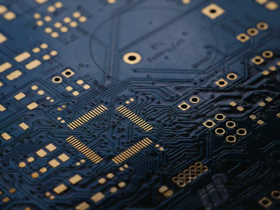
If you're looking for a PCB Fabrication Service partner who supports testing from bare PCB boards to assembled PCBA, start here: PCB Fabrication Service. Testing is not an “extra step” added at the end—it’s one of most important step of the PCB manufacturing process that verifies quality, yield, and reliability.
Modern electronics are getting dense and complex. A single open via, weak solder joint, or contamination issue can turn into intermittent failures that are hard to debug and even harder to reproduce. That’s why understanding the most common PCB testing methods—and how they fit together—matters whether you’re an PCB design engineer, purchase engineer, or project manager.
Section 1: Fundamentals of PCB Testing
What is PCB testing?
PCB testing is a set of inspection and measurement steps used to confirm that a printed circuit board meets design intention or not. Depending on the stage, the goal may be:
● Verify the bare board has correct connectivity and insulation
● Confirm the assembled board has correct component placement and solder integrity
● Validate the system function under real operating conditions
● Stress the product to uncover early-life or environment-triggered failures
Prototype vs. manufacturing testing
Prototype testing often prioritizes speed and learning:
● Catch gross shorts/opens quickly
● Validate core functionality
● Identify design errors before mass production
Manufacturing testing prioritizes consistency and coverage:
● Detect repeatable defects efficiently
● Reduce escapes (bad boards shipped)
● Provide traceability and compliance evidence
Key goals: functionality, reliability, compliance, cost efficiency
A practical testing strategy balances four goals:
● Functionality: does it work as intended?
● Reliability: will it keep working over time and stress?
● Compliance: does it meet standards/specs required by industry or customer?
● Cost efficiency: are we testing correctly and efficiently, not just testing more?
Overview of test categories
Most PCB testing methods are:
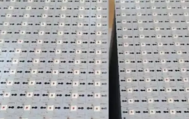
● Visual inspection: human or machine such as AOI
● Electrical tests: continuity/isolation/impedance
● Structural inspection: X-ray, microsections, solder joint analysis
● Functional tests: powering up and verifying outputs
● Environmental tests: temperature, humidity, vibration, cycling
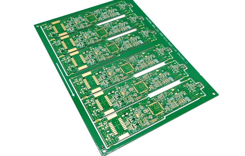
Section 2: Bare Board Testing
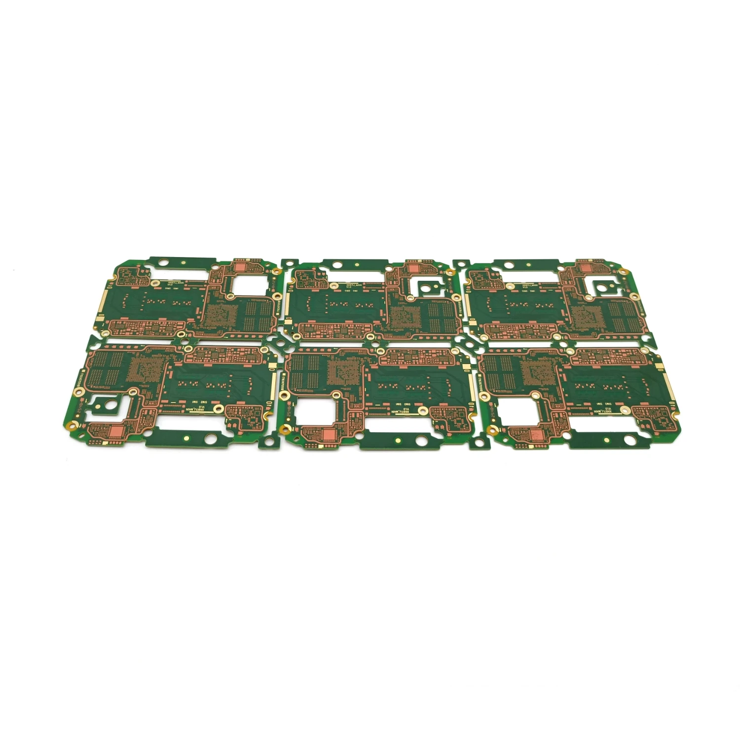
Bare board testing should be completed before components assembly, when the board is “just copper and laminate.” It’s one of the highest ROI steps in the PCB manufacturing process because it prevents you from building components onto a defective foundation.
Definition and importance
Bare board testing verifies:
● Net-to-net connections are correct (no opens)
● Unrelated nets are isolated (no shorts/leakage)
● Controlled impedance features meet targets (when required)
● Fabrication defects are caught before assembly adds cost
Key bare board tests
Visual inspection (manual and AOI-assisted)
Even basic checks can catch:
● Scratches, dents, exposed copper, solder mask defects
● Etching issues (over-etch/under-etch)
● Misregistration hints (annular ring problems)
● Surface finish anomalies
AOI-assisted inspection helps scale consistency and reduce human work(such as fatigue), especially on high-density patterns.
Electrical tests: continuity, isolation, impedance
Bare board electrical tests typically include:
● Continuity: confirms each net conducts where intended
● Isolation: confirms different nets are separated (high resistance between them)
● Impedance verification (when specified): checks controlled impedance traces using tools such as TDR (time-domain reflectometry) for transmission line behavior
Flying probe vs. bed-of-nails (fixture)
Two common ways to apply electrical tests:
● Flying probe: robotic probes move to test points without a dedicated fixture
● Bed-of-nails: a custom fixture contacts many points at once (fast per unit, upfront setup time)
Challenges: high-density boards, cost, time
As trace widths shrink and pads/vias get smaller:
● Contact points may be limited or non-existent
● Test access becomes harder
● Fixture probing may require tighter tolerances and better design-for-test (DFT)
How to choose based on volume & complexity
● Prototypes / low volume: flying probe is usually the practical choice
● High volume: bed-of-nails becomes cost-effective and faster per board
● High-density / limited access: consider a mix of bare board electrical + AOI + targeted impedance checks
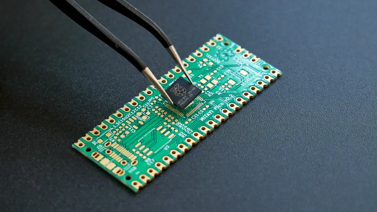
Section 3: In-Circuit Testing (ICT)
ICT is a kind of testing method for assembled PCB boards(PCBA), especially when you need results at scale.
What is ICT and how it works
In-Circuit Testing verifies component-level and net-level behavior on a populated PCB by probing test points, using a fixture (commonly bed-of-nails). It can measure:
● Resistance, capacitance, inductance (in-circuit)
● Diode junction behavior
● Shorts/opens on assembled nets
● Certain IC-level checks (limited by access and design)
Advantages
● Very fast once the fixture is built
● High repeatability and strong test coverage on accessible nodes
● Good at pinpointing faults (which net/component is out of spec)
Limitations
● Fixture cost and lead time (not ideal for frequent revisions)
● Limited access on dense boards (BGAs, tiny packages, minimal test pads)
● Doesn’t always validate “real function” (it validates electrical characteristics)
Ideal application cases
ICT shines for:
● High-volume manufacturing
● Boards with good test-point access
● Analog-heavy designs where passive values matter
● Products need consistent, fast screening
Fixtures and software control
A strong ICT program is not just hardware. It includes:
● Stable fixture design
● Well-maintained pins and contact force control
● Test software tuned for coverage, false-fail reduction, and fast cycle time
● Clear failure logging to assist and accelerate repair
Section 4: Flying Probe Testing (FPT)
Flying probe testing is often the go-to for prototypes and low-to-mid volume builds—especially when designs change frequently.
How it works
Flying probe systems use robotic needles to contact pads/vias/test points one by one based on CAD data. Because there’s no dedicated fixture, setup is largely software-driven.
Advantages for prototypes and low-volume runs
● No fixture cost or lead time
● Update program quickly when the design changes
● Useful when you have multiple product variants or frequent ECOs
Limitations
● Slower per board than ICT when go for high volume
● Coverage depends on access points and test program quality
● Very dense boards may still require alternative strategies (boundary scan, AXI, functional)
Best practices
● Probe path optimization to reduce moving time
● Test-point planning in the layout stage (even minimal pads help)
● Combine with AOI early to catch obvious placement/solder issues before electrical probing
Section 5: Functional Testing
Functional testing answers the question everyone cares about: “Does the board actually work well?”
Testing PCBs in real-world conditions
Functional testing typically need to powering on the PCB (or PCBA) and verifying:
● Power voltage and current are within expected range
● Communication interfaces work (USB, UART, CAN, Ethernet, etc.)
● Sensors/actuators respond correctly
● Firmware boots and runs stable routines
● Output signals meet expected behavior
Manual vs automated functional tests
● Manual: flexible, good for prototypes, but slow at scale
● Automated: repeatable and faster for production; requires development effort and fixtures (not necessarily bed-of-nails, could be pogopin interfaces, connectors, harnesses)
Strengths and weaknesses
Functional tests are essential, but they can be “black-box”:
● They confirm function
● They may not pinpoint the exact failing component or joint without additional diagnostics
Integration with other tests
The best approach:
● Bare board test prevents foundational defects on PCB
● AOI/AXI find structural/assembly issues
● ICT/FPT pinpoint electrical opens/shorts and component-level problems
● Functional testing verifies real working status
Section 6: Automated Optical Inspection (AOI)
AOI is a visual inspection method that uses cameras and software to compare the board against expected patterns.
How AOI works
High-resolution images are captured and analyzed:
● Compare placement position, rotation, polarity marks
● Detect solder anomalies (depending on AOI capability)
● Identify missing/incorrect components
Detectable defects
AOI commonly spots:
● Missing components
● Wrong orientation (diodes, ICs, electrolytics)
● Offset placement and tombstoning
● Solder bridging and insufficient solder (to a degree)
● Silkscreen and marking mismatches that hint at process issues
Why AOI is valuable in the production line
AOI works best as an “early filter”:
● Spot issues right after placement/reflow(Physical and visual)
● Reduce the load on later electrical tests(functional)
● Improve feedback loops to stencil, placement, and reflow processes(feedback loop for the prior process)
Section 7: X-Ray Inspection (AXI)
AOI is inspecting the physical appearance by visual, and X-ray is “penetrating view” —especially for the inside of components, where with covers that you can’t see.
Why X-ray matters for hidden joints
Packages like BGA and LGA hide solder connections under the component body. X-ray inspection helps evaluate:
● Solder voiding
● Bridging under the package
● Misalignment
● Incomplete joints
Imaging and analysis process
AXI systems capture radiographic images and apply analysis rules to quantify:
● Joint shape and consistency
● Void area trends
● Alignment and ball collapse patterns
Complementing other tests
AXI pairs well with:
● ICT/FPT: electrical confirmation where accessible
● Functional test: system-level validation
● Process control: monitoring voiding trends, reflow stability, and stencil performance
Section 8: Advanced Testing Methods
As products move into high-speed, high-reliability, or regulated categories, additional methods become common.
Stress testing
Stress testing runs PCB boards under controlled stress (heat, load, time) to accelerate aging and bust early-life failures. It’s useful when:
● Want to find out the weak components before releasing to market
● The electronic product will be working continuously or sometimes in harsh environments
ROSE testing (resistivity of solvent extract)
ROSE checks ionic contamination from flux residues and handling. This matters when:
● High impedance circuits are sensitive to leakage
● Long-term corrosion risk must be minimized
● Failures show up later as intermittent behavior
Boundary scan (JTAG)
Boundary scan is valuable when physical probing access is limited (dense BGAs, minimal test pads). It can:
● Verify interconnects between digital devices
● Provide a fixture-light method to improve coverage
Impedance and high-frequency signal testing
For high-speed boards, “continuity” isn’t enough. You may need:
● Controlled impedance verification (TDR)
● Insertion loss/return loss checks (for demanding RF/high-speed channels)
● Signal integrity validations in targeted scenarios as part of engineering qualification
Section 9: Environmental Testing
● Temperature, humidity, vibration, thermal cycling
● Ensuring reliability under operating conditions
● Industry compliance examples: AS9100, IPC, MIL-STD
Section 10: How to Choose the Right PCB Testing Strategy
There is no single “best” testing method. The right strategy depends on what is needed and what failure would cost you.
Key factors
● Design complexity: density, pitch, BGAs, HDI, controlled impedance
● Volume: prototypes vs mass production
● Budget and schedule: fixture lead time vs test cycle time
● Application risk: consumer gadget vs medical/industrial/automotive
● Test access: availability of pads, connectors, boundary scan support
Combining methods for optimal coverage
A common layered strategy looks like:
● Bare board test (electrical + AOI where needed)
● AOI after assembly
● ICT (high volume) or flying probe (low volume)
● AXI for hidden joints
● Functional test for real behavior
● Environmental/burn-in for high reliability products
Cost-effective tips that actually work
● Add test points early—tiny pads can save enormous time later
● Use AXI selectively (target critical BGAs/power modules)
● Don't rely on functional test alone if you need root-cause speed
● Treat testing as process feedback, not just pass/fail
Decision guide table (volume vs method vs typical use)
Production Volume | Best-Fit Methods | Why It Works | Watch Outs |
Prototype (1–20) | FPT + AOI + basic functional | Fast setup, flexible for revisions | Limited access can reduce coverage |
Low–Mid (20–1,000) | FPT or light ICT + AOI + functional | Balanced speed and cost | Consider AXI if BGAs are critical |
High Volume (1,000+) | ICT + AOI + functional (plus AXI as needed) | High throughput, repeatable screening | Fixture build time, DFT required |
High-Reliability | Add burn-in / environmental + contamination checks | Catches latent failures | Requires planning, data discipline |
Section 11: Case Studies
Example 1: Class 3 prototype tested with FPT + AOI
Scenario: A dense prototype with fine-pitch components and limited test pads.
Approach:
● AOI after reflow to spot polarity/placement issues early
● Flying probe to confirm opens/shorts without fixture
● Targeted functional checks to validate core behavior
Result:
● Faster debug because faults had been identified prior
● Reduce time for chasing “firmware issues” that were actually solder/placement errors
Example 2: Mass production PCB, tested by ICT + functional test + AXI
Scenario: A stable design moving into high-volume production, including BGAs.
Approach:
● ICT for high-coverage electrical screening and isolation of defects
● Functional test to validate real operation under controlled input/output conditions
● AXI sampling or full coverage for critical BGA joints
Result:
● Higher yield stability through consistent screening
● Lower escape rate due to hidden-joint visibility
● Faster actions to correct workflow&process when trends appeared (voiding, placement drift, reflow profile drift)
Section 12: FAQs
What is the difference between AOI and ICT?
AOI is for visual pattern inspection; ICT is electrical probing and measurement. AOI spots placement and visible solder issues. ICT catches connectivity/component value issues where access exists.
Can I skip bare board testing for prototypes?
You can, but it’s risky. If a bare board has an open or short, you’ll waste time debugging an assembled board and may not possible to repair it if there are issue in inner layer.
How do I test PCBs with BGAs or fine-pitch components?
Combine methods:
● AOI for placement
● AXI for hidden joints
● Boundary scan if supported
● Functional tests for working performance
● Add test points or dedicated test connectors where possible
How often should functional testing be performed?
Typically every unit in production, but different when:
● Full functional for mission-critical products
● Reduced functional plus statistical sampling for lower-risk designs (depending on quality targets)
What’s the cost difference between flying probe and bed-of-nails?
Flying probe has lower setup cost and fast to changeover, but slower per board. Bed-of-nails requires fixture investment, but is much faster per board at high volume. The break-even depends on volume, complexity, and revision frequency.
Section 13: Conclusion
No single test is applicable for everything. The most reliable products come from a combined approach where PCB testing methods support each other:
● Bare board testing prevents foundational defects, especially inner layer
● AOI and AXI reveal assembly issues (including hidden joints)
● ICT or flying probe validates electrical integrity at scale or during prototyping
● Functional testing confirms the product works correctly
● Environmental and advanced tests reduce long-term failure risk
In the end, testing is not separated from manufacturing—it’s part of the PCB manufacturing process itself. When testing is planned at early stage (DFT, test points, inspection strategy), it lowers cost and improves the quality.
If you want a partner who can support both fabrication and test methods—from bare PCB boards to assembled PCBA—Benlida is very good at them, combine testing process into the workflow so the quality of each PCB&PCBA could be verified and validated.
Related PCB manufacturing processes
PCB Manufacturing Process Step-by-Step
PCB Inner Layer Imaging & Etching Process
What is the PCB Lamination Process?
How do drilling (mechanical/laser) processes work in PCB manufacturing?
What is the plating process in PCB Manufacturing?
How are vias formed in PCBs?
How is solder mask applied on PCB?
Ultimate Guide to PCB silk screen printing process
What is the surface finish process in PCB?
About the auther:

Sonic Yang
As a major of Electronics and Mechanical Automation, Sonic has been engaged in PCB design, R&D, manufacturing of eletronics for around 22 years, as engineering director and coordinates with supply chain(components&CNC parts), providing professional supports and consults for global customers.
 en
en

 WhatsApp